A signal amplification structure and communication equipment
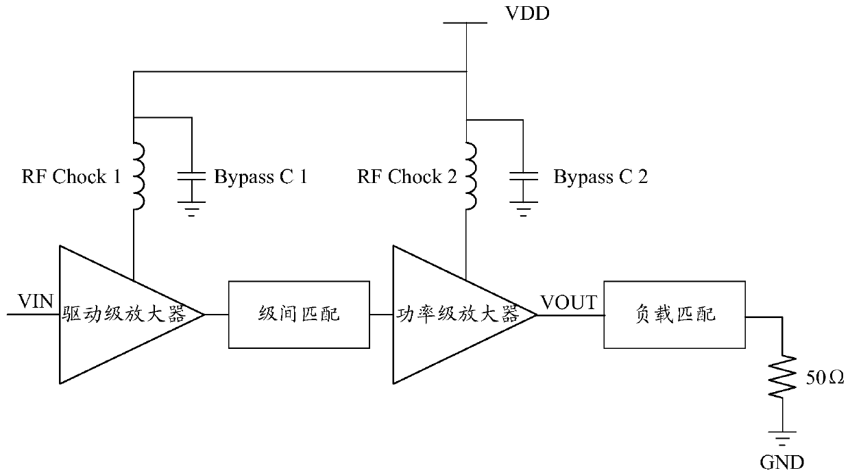
A signal amplification and amplifier technology, applied in the field of wireless communication design, can solve problems such as complex circuits, unstable power amplification, redundancy, etc., and achieve the effect of suppressing oscillation frequency and improving stability
- Summary
- Abstract
- Description
- Claims
- Application Information
AI Technical Summary
Problems solved by technology
Method used
Image
Examples
Embodiment 1
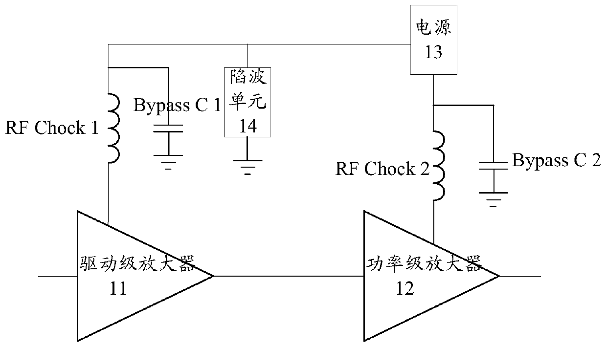
[0021] An embodiment of the present invention provides a signal amplification structure. figure 2 It is a schematic diagram of the composition structure of the signal amplification structure of the embodiment of the present invention; as figure 2 As shown, the signal amplification structure includes: at least one driver amplifier 11 and a power amplifier 12; the at least one driver amplifier 11 is connected in series; the at least one driver amplifier 11 and the power amplifier 12 are connected to the same A power supply 13, making the at least one driver stage amplifier 11 respectively form a loop with the power stage amplifier 12;
[0022] The signal amplifying structure further includes a notch unit 14 for blocking the oscillation frequency in the loop; one end of the notch unit 14 is connected to the loop, and the other end of the notch unit 14 is grounded. figure 2 In the above, the signal amplification structure includes a driver amplifier 11 and a power amplifier 12...
Embodiment approach
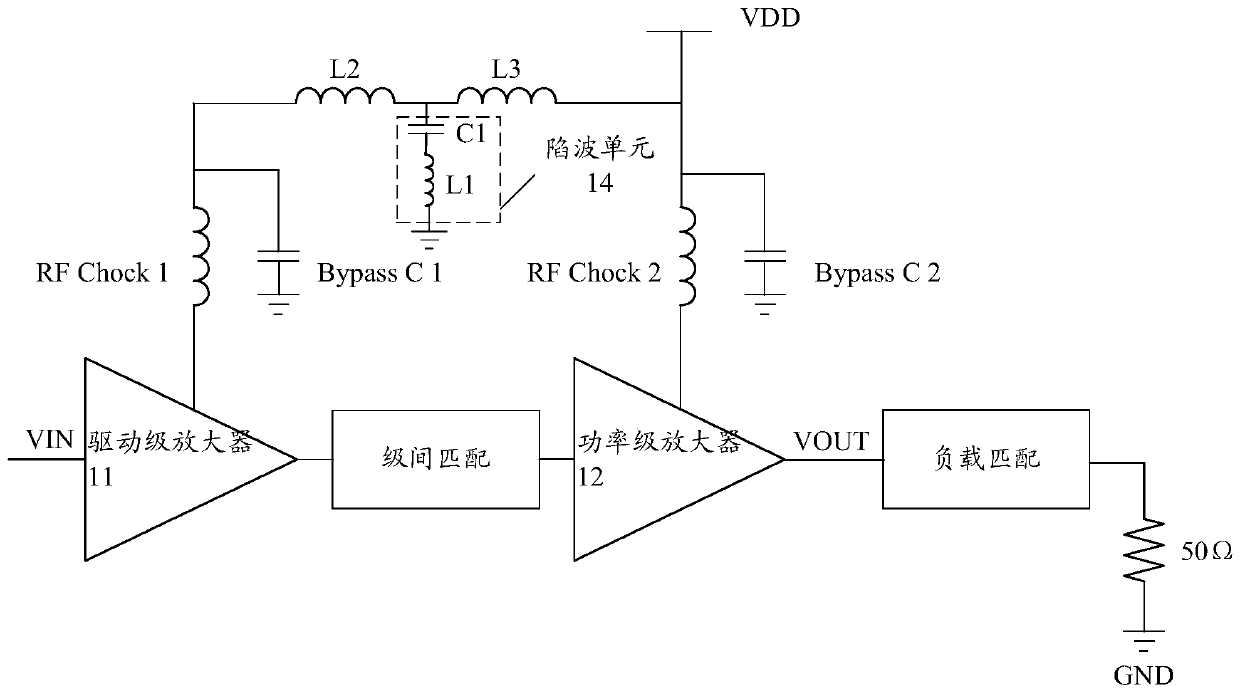
[0026] Specifically, the notch unit 14 may be composed of a first capacitor C1 and a first inductance L1; the values of the first capacitor C1 and the first inductance L1 in the notch unit 14 are determined according to the oscillation frequency generated in the loop. Specifically, the capacitance value of the first capacitor C1 and the inductance value of the first inductor L1 are adapted to the oscillation frequency in the loop. As an implementation manner, the relationship between the capacitance value of the first capacitor C1, the inductance value of the first inductor L1 and the oscillation frequency in the loop satisfies:
[0027] Wherein, f is the oscillation frequency; L is the inductance value of the first inductor L1; C is the capacitance value of the first capacitor C1.
[0028] As an implementation manner, the first low-pass filtering unit includes a second inductor L2 and the first capacitor C1; the second inductor L2 is connected in series in the first loop;...
Embodiment 2
[0033]The embodiment of the present invention also provides a communication device, the communication device includes the signal amplification structure according to the first embodiment of the present invention. Specifically, such as figure 2 As shown, the signal amplification structure includes: at least one driver amplifier 11 and a power amplifier 12; the at least one driver amplifier 11 is connected in series; the at least one driver amplifier 11 and the power amplifier 12 are connected to the same A power supply 13, making the at least one driver stage amplifier 11 form a loop with the power stage amplifier 12 respectively;
[0034] The signal amplifying structure further includes a notch unit 14 for blocking the oscillation frequency in the loop; one end of the notch unit 14 is connected to the loop, and the other end of the notch unit 14 is grounded.
[0035] In the embodiment of the present invention, in order to satisfy the wireless communication quality of the com...
PUM
 Abstract
Description
Claims
Application Information


