White light-emitting device and manufacturing method thereof
A light-emitting device, white light technology, applied in the direction of semiconductor devices, electrical components, circuits, etc., can solve the problems of uneven light emission, low light-emitting purity, weak reflection of inorganic phosphors, etc., and achieve the effect of high light-purity and uniform light-emitting
- Summary
- Abstract
- Description
- Claims
- Application Information
AI Technical Summary
Problems solved by technology
Method used
Image
Examples
Embodiment 1
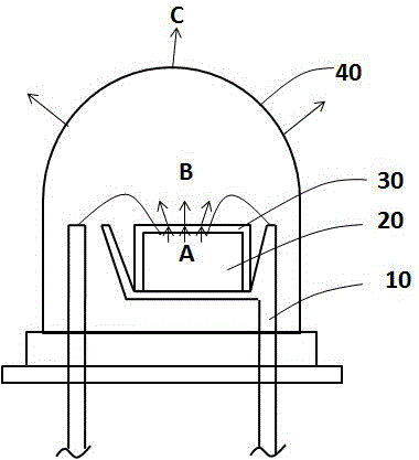
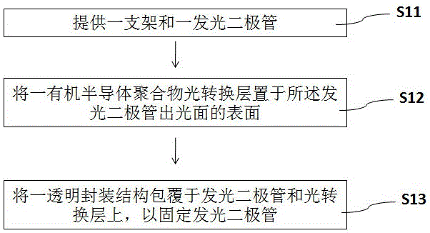
[0025] See attached figure 1 , a schematic cross-sectional view of a white light emitting device according to an embodiment of the present invention. The white light emitting device provided by the present invention includes a support 10, a light-emitting diode 20 on the support 10, an organic semiconductor polymer light conversion layer 30, and a transparent encapsulation structure 40 for protecting and fixing the light-emitting diode 20. The light conversion layer 30 absorbs The first light A emitted by the light emitting diode 20 is converted into a second light B different from the first light A, and the first light A and the second light B are mixed in the transparent encapsulation structure 40 to form white light C. Wherein, the material of the transparent encapsulation structure 40 is an encapsulation resin; the material of the organic semiconducting polymer light conversion layer 30 is a thiophene polymer, especially a high isotactic poly-3-hexylthiophene. In some embo...
Embodiment 2
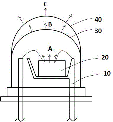
[0034] The difference between this embodiment and Embodiment 1 is that the organic semiconducting polymer light conversion layer 30 is disposed in the transparent encapsulation structure 40, and the transparent encapsulation structure 40 with the built-in organic semiconducting polymer light conversion layer 30 covers the light emitting diode 20 to protect and Fix the light emitting diode 20 .
[0035] The method for making the above-mentioned light-emitting diodes in this embodiment specifically includes the following steps:
[0036] S21, providing a bracket 10 and a light emitting diode 20;
[0037] S22, arranging an organic semiconductor polymer light conversion layer 30 in a transparent encapsulation structure 40;
[0038] S23 , covering the light-emitting diode 20 with the transparent encapsulation structure 40 built with the organic semiconductor polymer light conversion layer 30 , so as to protect and fix the light-emitting diode 20 .
[0039] Wherein, the organic sem...
PUM
 Abstract
Description
Claims
Application Information


