Nanowire semiconductor device and formation method thereof

一种半导体、纳米线的技术,应用在纳米线半导体器件及其形成领域,能够解决难以保证器件性能及其稳定性等问题,达到表面圆滑、分布均匀、改善性能的效果

Active Publication Date: 2017-06-16
SEMICON MFG INT (BEIJING) CORP +1
View PDF3 Cites 2 Cited by
  • Summary
  • Abstract
  • Description
  • Claims
  • Application Information

AI Technical Summary

Problems solved by technology

[0004] However, the nanowire semiconductor devices formed in the prior art are difficult to guarantee the performance and stability of the device

Method used


Image

  • Nanowire semiconductor device and formation method thereof
  • Nanowire semiconductor device and formation method thereof
  • Nanowire semiconductor device and formation method thereof

Examples


Embodiment Construction

[0041] It can be seen from the background art that the nanowire semiconductor devices formed in the prior art have the problem of poor performance. The reasons for the poor performance are analyzed in combination with the formation process of nanowire semiconductor devices:

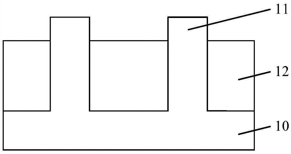
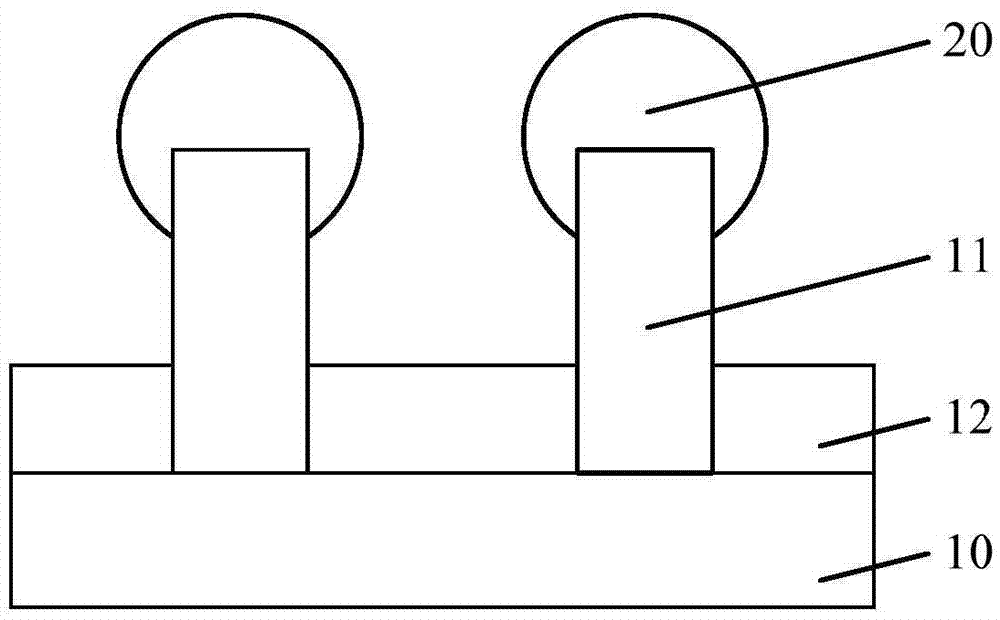
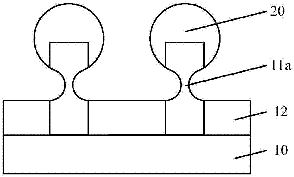
[0042] refer to Figure 1 to Figure 4 , is a schematic structural view showing various steps of a method for forming a nanowire semiconductor device in the prior art.

[0043] refer to figure 1 , providing a silicon substrate 10 . The substrate 10 is etched to form fins 11 , and an isolation layer 12 is formed between adjacent fins 11 .

[0044] refer to figure 2 A SiGe epitaxial line 20 is formed on the top of the fin portion 11 by selective epitaxy. Afterwards, the isolation structure 12 is etched back to expose part of the side surfaces of the fins 11 .

[0045] refer to image 3 , removing part of the thickness of the side of the fin 11 , so that the side of the fin 11 is necked-in.

[0046] ...


PUM


Abstract

The invention provides a nanowire semiconductor device and a formation method thereof. The formation method thereof comprises the following steps: forming a substrate; forming a first opening in the substrate of a PMOS region; filling a germanium-silicon material in the first opening of the PMOS region to form a first epitaxial wire; etching the bottom portion of the first epitaxial wire and the substrate at the two sides to enable the first epitaxial wire to be located at the side wall of a second opening and suspended at the bottom portion of the second opening; carrying out thermal oxidation treatment on the first epitaxial wire and removing oxide formed on the surface of the first epitaxial wire in the thermal oxidation treatment process to form a first nano wire; and forming a first ring-fence structure. The first opening is directly filled with the germanium-silicon material to form the first epitaxial wire, so that distribution the germanium-silicon material in the first epitaxial wire is relatively uniform, germanium content in the first nano wire is improved through the thermal oxidation treatment process, channel performance of the formed semiconductor device is improved favorably, and performance of the semiconductor device is improved.

Description

technical field [0001] The invention relates to the field of semiconductor manufacturing, in particular to a nanowire semiconductor device and a forming method thereof. Background technique [0002] With the rapid development of semiconductor manufacturing technology, semiconductor devices are developing towards higher component density and higher integration. Transistors, as the most basic semiconductor devices, are currently being widely used. Therefore, as the component density and integration of semiconductor devices increase, the size of transistors is also getting smaller and smaller. The problems of short channel effect and gate leakage current in small size make the performance of transistor worse, so it faces a series of difficulties to improve performance by shrinking the physical size of traditional transistors. [0003] In order to solve the difficulty of further reducing the physical size of traditional semiconductor devices, a nanowire semiconductor device is ...

Claims


Application Information

Patent Timeline
Patent Type & Authority Applications(China)
IPC IPC(8): H01L29/78H01L21/336
CPCH01L29/66795H01L29/785H01L29/775H01L29/78684H01L29/1054H01L29/66439H01L21/823807H01L29/0673H01L29/267H01L29/42392H01L29/78696H01L21/02236H01L21/31105H01L21/8252H01L21/8258H01L21/84H01L27/1222H01L27/1225H01L29/161H01L29/20H01L29/66522H01L29/66742
Inventor 肖德元
Owner SEMICON MFG INT (BEIJING) CORP
Why Eureka
Try Eureka