A three-dimensional memory readout circuit and readout method

A readout circuit and three-dimensional storage technology, which is applied in the field of integrated circuits, can solve problems such as long readout time, high complexity, and misreading, so as to reduce readout time, eliminate false readouts, and reduce misreadouts Effect

Active Publication Date: 2019-05-14
SHANGHAI INST OF MICROSYSTEM & INFORMATION TECH CHINESE ACAD OF SCI
View PDF4 Cites 0 Cited by
  • Summary
  • Abstract
  • Description
  • Claims
  • Application Information

AI Technical Summary

Problems solved by technology

[0004] Three-dimensional memory is different from two-dimensional memory. In two-dimensional memory, parasitic devices are mainly in the plane direction, while in three-dimensional memory, parasitic devices exist in both vertical and plane directions. The number and complexity of parasitic parameters in three-dimensional memory are far greater than Two-dimensional memory; at the same time, the three-dimensional memory adopts a new type of gating device, which needs to increase the unselected bit line and unselected word line. The bias method of the three-dimensional memory is completely different from that of the two-dimensional memory, and the complexity is higher; in addition, due to The unique biasing method of 3D memory will cause leakage current
[0010] Four, leakage
If the leakage of the half-gated memory cell is small (such as 5pA), the leakage will cause false reading and affect the reading speed
[0011] Therefore, how to improve the above-mentioned long reading time and how to improve the speed characteristics of the three-dimensional memory has become a technical problem to be solved urgently by those skilled in the art.

Method used


Image

  • A three-dimensional memory readout circuit and readout method
  • A three-dimensional memory readout circuit and readout method
  • A three-dimensional memory readout circuit and readout method

Examples


Embodiment 1

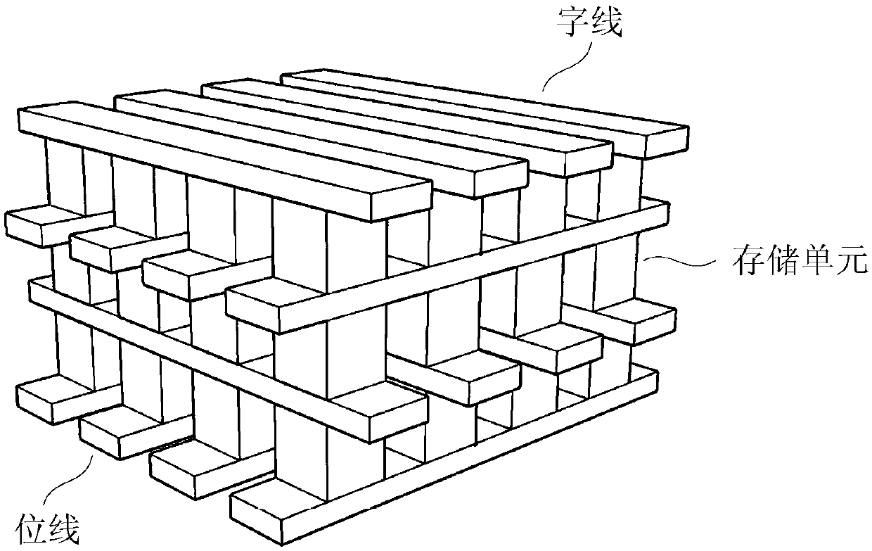
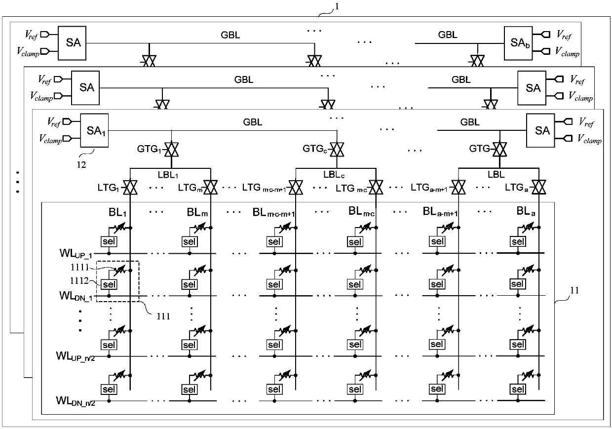
[0085] Such as Figure 3 ~ Figure 5 As shown, the present invention provides a three-dimensional memory readout circuit, which includes a three-dimensional memory cell array 1 and a read reference circuit 2 .

[0086] Such as image 3 As shown, the three-dimensional memory cell array 1 includes at least one three-dimensional memory cell sub-array 11 and a plurality of sense amplifiers 12 corresponding to the three-dimensional memory cell sub-array, and each bit line in the three-dimensional memory cell array 1 respectively passes through the transmission gate It is connected with the corresponding sense amplifier 12; the sense amplifier 12 is connected with the read reference circuit 2 and the corresponding memory cell, and compares the read reference current with the current read in the selected memory cell to generate the selected memory cell The read voltage signal of the cell.

[0087] Specifically, such as image 3 As shown, in this embodiment, the three-dimensional me...

Embodiment 2

[0107] Such as Figure 6 As shown, this embodiment provides a three-dimensional memory readout circuit, the structure of the three-dimensional memory readout circuit is similar to that of Embodiment 1, the difference is that the three-dimensional memory readout circuit further includes: connected to the reference The word line matching module between the word line W1' and the unselected bit line DESBL is used to provide the leakage on the word line to match the leakage of the storage cells on the word line in the three-dimensional memory cell array 1 .

[0108] Specifically, such as Figure 6 As shown, the word line matching module 28 includes (a-1) memory cells connected in parallel, where a is the number of bit lines connected to the same word line in the three-dimensional memory cell array 1 .

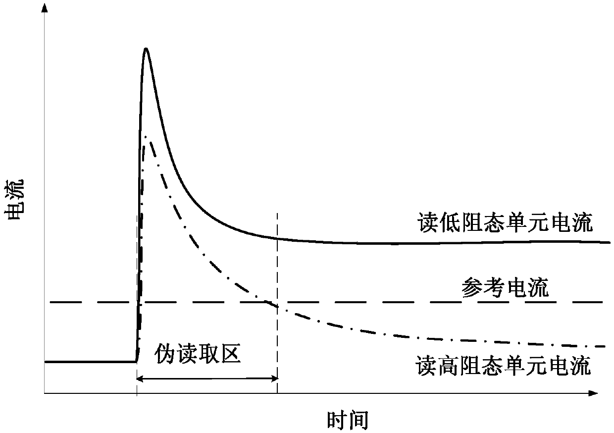
[0109] Correspondingly, the first clamping transistor 26 is based on the reference resistance value, the bit line parasitic parameters and the leakage current provided by the bit l...


PUM


Abstract

The invention provides a three-dimensional memory readout circuit and a readout method, comprising: a read reference circuit for generating a read reference current capable of quickly distinguishing between reading a low-resistance state cell current and a high-resistance state cell current; and a sensitive amplifier. The reading reference circuit includes a reference unit, a bit line matching module, a word line matching module and a transmission gate parasitic parameter matching module. The invention aims at the parasitic effect and electric leakage of the three-dimensional memory in the plane and vertical directions, introduces the matching of the parasitic parameters of the bit line, electric leakage and transmission gate in the reading reference current, and introduces the matching of the parasitic parameters of the current mirror in the reading current, eliminating Pseudo-read phenomenon reduces the read-out time; and has a wide range of applications and a high read-out accuracy rate.

Description

technical field [0001] The invention relates to the technical field of integrated circuits, in particular to a three-dimensional memory readout circuit and a readout method. Background technique [0002] Integrated circuit memory is widely used in industrial and consumer electronics products, and can be divided into volatile memory and non-volatile memory according to whether the memory can be stored when power is off. Non-volatile memory includes flash memory (flash memory), magnetic memory (magnetoresistive random-access memory, MRAM), resistive random-access memory (resistance random-access memory, RRAM), phase change memory (phase change memory, PCM), etc. Phase-change memory is a memory based on the Ovsinski electronic effect proposed by Ovsinski in the late 1960s. Different resistance states in the high resistance state (amorphous state) are used to store data. Magnetic memory and RRAM also use different resistance states of materials or devices in low resistance sta...

Claims


Application Information

Patent Timeline
Patent Type & Authority Patents(China)
IPC IPC(8): G11C5/02G11C7/06G11C7/10
CPCG11C5/02G11C7/062G11C7/1051G11C13/004G11C2013/0045G11C2013/0054G11C13/003G11C13/0026G11C13/0004G11C2213/71G11C13/0038G11C13/0061G11C13/0028
Inventor 雷宇陈后鹏宋志棠
Owner SHANGHAI INST OF MICROSYSTEM & INFORMATION TECH CHINESE ACAD OF SCI
Why Eureka
Try Eureka