Nonvolatile memory readout circuit and readout method

A technology of non-volatile memory and readout circuit, which is applied in the field of integrated circuits and can solve the problems of long readout time and large dynamic power consumption of non-volatile memory

Active Publication Date: 2021-04-13
SHANGHAI INST OF MICROSYSTEM & INFORMATION TECH CHINESE ACAD OF SCI
View PDF4 Cites 0 Cited by
  • Summary
  • Abstract
  • Description
  • Claims
  • Application Information

AI Technical Summary

Problems solved by technology

[0007] In view of the shortcomings of the prior art described above, the purpose of the present invention is to provide a non-volatile memory readout circuit and a readout method, which are used to solve the problem of excessively long readout time and dynamic power consumption of the non-volatile memory in the prior art. Too big and other problems

Method used


Image

  • Nonvolatile memory readout circuit and readout method
  • Nonvolatile memory readout circuit and readout method
  • Nonvolatile memory readout circuit and readout method

Examples


Embodiment 1

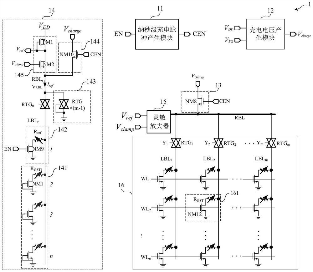
[0090] Such as figure 2 As shown, the present embodiment provides a non-volatile memory readout circuit 1, and the non-volatile memory readout circuit 1 includes: a nanosecond charge pulse generating module 11, a charging voltage generating module 12, and a bit line charging module 13. A first reference read voltage generating circuit 14 and a sense amplifier 15.

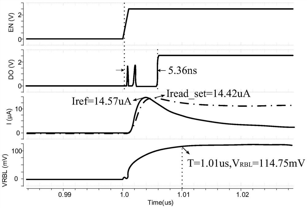
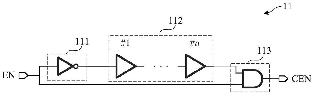
[0091] Such as figure 2 As shown, the nanosecond charging pulse generation module 11 receives the read enable signal EN, and generates a post-charge pulse signal CEN after the read enable signal EN arrives.

[0092] Specifically, in this embodiment, the sustaining time of the post-charging pulse signal CEN is set to 100 ps-10 ns. In actual use, the sustaining time of the post-charging pulse signal CEN can be set according to circuit performance and needs. It is not limited to this embodiment.

[0093] Specifically, such as image 3 As shown, in this embodiment, the nanosecond charging pulse generation module 1...

Embodiment 2

[0124] Such as Figure 2 ~ Figure 6 As shown, this embodiment provides a method for reading out a non-volatile memory, and the method for reading out a non-volatile memory includes:

[0125] After the read enable signal EN is valid, the read operation starts, a word line and a bit line are selected, and a post-charging pulse signal CEN is generated at the same time.

[0126] At the same time when the read enable signal EN is valid, the read current Vread of a selected memory cell in the memory array 16 is read.

[0127] At the same moment when the read enable signal EN is valid, the read bit line is charged based on the post charge pulse signal CEN.

[0128] At the same moment when the read enable signal EN is effective, the reference read bit line is charged based on the post-charge pulse signal CEN to generate a dynamic reference read current Iref, and the reference read current Iref is the same as the read current Iread The transient curves of the reference read current I...


PUM


Abstract

The invention provides a nonvolatile memory readout circuit and a readout method, comprising: a nanosecond-level charging pulse generation module, which generates a post-charging pulse signal; a charging voltage generation module, which generates a post-charging voltage; and a charging module for reading bit lines, which provides The read bit line is charged; the first reference read voltage generating circuit charges the reference read bit line and generates a reference read current and a first reference read voltage; a sense amplifier compares the reference read current with the read current to generate a read voltage Signal. The invention improves the rising speed of the read bit line voltage, reduces the peak value of the read current, reduces the dynamic power consumption, and reduces the time required for the read current and the reference read current to reach a stable value; The matching of parasitic parameters introduces the matching of the parasitic parameters of the current mirror in the read current, and performs post-charging operation on the read bit line and the read reference bit line, which eliminates the false read phenomenon to the greatest extent and reduces the read time.

Description

technical field [0001] The invention relates to the technical field of integrated circuits, in particular to a nonvolatile memory readout circuit and a readout method. Background technique [0002] In the field of integrated circuit manufacturing, as the process nodes continue to shrink, traditional charge-based memories are increasingly limited. Various new memories and new structures have been invented to break through the original limits: MLC NAND, MLC NOR, TLC NAND, MRAM, RRAM, FeRAM, 3D-Xpoint, 3D-NAND, etc. The read latency of traditional and new memories is different: for SRAM as memory, the read time of DRAM is within 10ns, that of NAND Flash is around 50us, that of 3D-NAND is around 500us, and that of hard disk is around 10ms. If the read time of the memory can be further mined, its competitiveness will be greatly improved. [0003] Phase Change Memory (Phase Change Memory, PCM) is a memory based on the Ovshinsky electronic effect proposed by Ovshinsky in the late...

Claims


Application Information

Patent Timeline
Patent Type & Authority Patents(China)
IPC IPC(8): G11C16/24G11C16/26
CPCG11C16/24G11C16/26
Inventor 雷宇陈后鹏宋志棠
Owner SHANGHAI INST OF MICROSYSTEM & INFORMATION TECH CHINESE ACAD OF SCI
Why Eureka
Try Eureka