Semiconductor wafer box particle detection method

A particle detection and semiconductor technology, applied in the field of semiconductor wafer box particle detection, can solve problems such as affecting the electrical performance of integrated circuits, reducing product yield, and product quality loss.

Inactive Publication Date: 2017-06-27
GRINM SEMICONDUCTOR MATERIALS CO LTD
View PDF2 Cites 3 Cited by
  • Summary
  • Abstract
  • Description
  • Claims
  • Application Information

AI Technical Summary

Problems solved by technology

[0003] The surface particles on the surface of the silicon wafer will affect the electrical properties of the integrated circuit. The silicon wafer with too many particles will form epitaxial surface defects in the subsequent processing of epitaxy, or in the process of the device. Short circuit, which leads to loss of product quality and lower product yield

Method used


Image

  • Semiconductor wafer box particle detection method
  • Semiconductor wafer box particle detection method

Examples


Embodiment

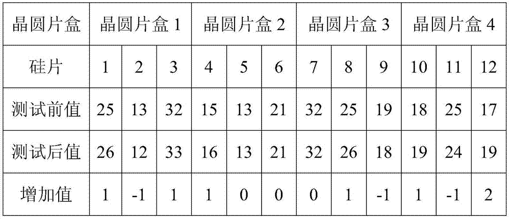
[0024] This embodiment is described by taking a 12-inch silicon wafer box that can hold 25 wafers as an example.

[0025] 1. Take 12 pieces of 12inch polished silicon wafers and 4 wafer boxes (front opening wafer box or wafer transport box (FOUP / FOSB));

[0026] 2. Use the surface particle tester KLA Tencor SP1 to test the surface particles of 12 pieces of 12inch polished silicon wafers, and record the previous value of the data;

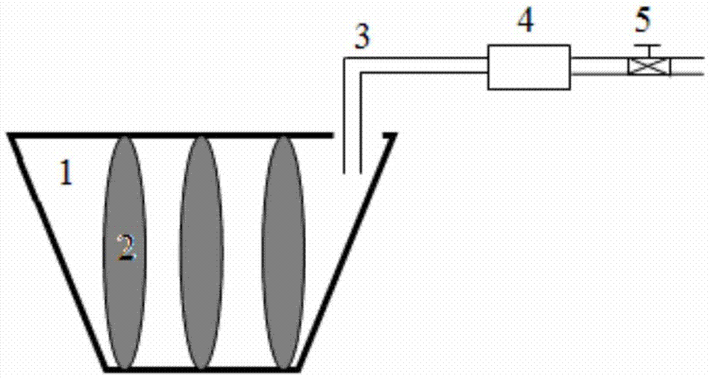
[0027] 3. Divide 12 pieces of 12inch polished silicon wafers into four groups, put them into the two ends and middle positions of 4 wafer cassettes (FOUP / FOSB) respectively, cover the wafer cassettes halfway, leave a certain gap, and then place them separately Put the air tube into the gap between the four wafer cassettes (be careful not to touch the silicon wafer), turn on the switch, and blow air for 1 minute each;

[0028] 4. Take out 12 pieces of 12inch polished silicon wafers, and then use the surface particle tester KLA Tencor SP1 to test the...


PUM


Abstract

The invention discloses a semiconductor wafer box particle detection method. The method comprises the following steps: (1) clean silicon wafers are prepared, and the number of particles on the surface of each silicon wafer is tested by using a particle testing instrument and recorded; (2) the clean silicon wafers are put to a to-be-tested wafer box, an air source blows and sweeps the inner part of the to-be-tested wafer box through an air path with a particle filter, the air pressure is about 15 to 30 psi, and blowing and sweeping of the air source are kept for 1 min; and (3) the particle testing instrument is used for testing the data of the particles on the surface of the silicon wafer, data are recorded, before-after added values are compared, and the semiconductor-used wafer box cleanness is judged. The wafer box particle cleanness can be detected in a quick, high-efficiency and batch mode, whether the wafer box particles are clean can be tested and analyzed timely, and the semiconductor silicon wafer can be ensured not to be polluted by the wafer box particles.

Description

technical field [0001] The invention relates to a particle detection method for a semiconductor wafer box, belonging to the technical field of silicon wafer processing. Background technique [0002] In recent years, the usage rate of silicon wafers for semiconductors has become higher and higher, and the amount of silicon wafers has also increased, and the size of silicon wafers has gradually increased to 12 inches or even 18 inches. However, the integration degree of silicon chips used in semiconductor integrated circuits increases, the line width decreases, and the requirements for the quality of silicon chips become more and more stringent. The quality parameters of silicon wafers mainly include surface particles or defects, surface metal content, internal metal (FE) content, minority carrier lifetime, diffusion length and other parameters. During the production and processing of silicon wafers, the performance of these parameters must be strictly monitored and analyzed. ...

Claims


Application Information

Patent Timeline
Patent Type & Authority Applications(China)
IPC IPC(8): H01L21/66G01N33/00
CPCG01N33/00G01N2033/0081H01L22/12H01L22/20
Inventor 赵而敬曹孜刘建涛李宗峰盛方毓冯泉林闫志瑞
Owner GRINM SEMICONDUCTOR MATERIALS CO LTD
Why Eureka
Try Eureka