
Manufacturing method of crystal oscillator element and crystal oscillator element

A manufacturing method and crystal oscillator technology, which is applied in the field of communication, can solve problems such as increased manufacturing costs, achieve the effects of reducing manufacturing costs, avoiding manual tin addition, and improving quality

Inactive Publication Date: 2017-06-27
ZHUHAI GOTECH INTELLIGENT TECH
View PDF4 Cites 2 Cited by
  • Summary
  • Abstract
  • Description
  • Claims
  • Application Information

AI Technical Summary

Problems solved by technology

[0004] The embodiment of the present invention provides a method for manufacturing a crystal oscillator component and the crystal oscillator component, which are used to solve the problem in the prior art that adding tin to the shell of the crystal oscillator requires manual tinning, which increases the manufacturing cost.

Method used


Image

  • Manufacturing method of crystal oscillator element and crystal oscillator element
  • Manufacturing method of crystal oscillator element and crystal oscillator element
  • Manufacturing method of crystal oscillator element and crystal oscillator element

Examples


Embodiment Construction

[0026] The technical solutions of the present invention will be described in detail below through the accompanying drawings and specific embodiments. It should be understood that the embodiments of the present invention and the specific technical features in the embodiments are only descriptions of the technical solutions of the present invention, rather than limitations. , the embodiments of the present invention and specific technical features in the embodiments may be combined with each other.

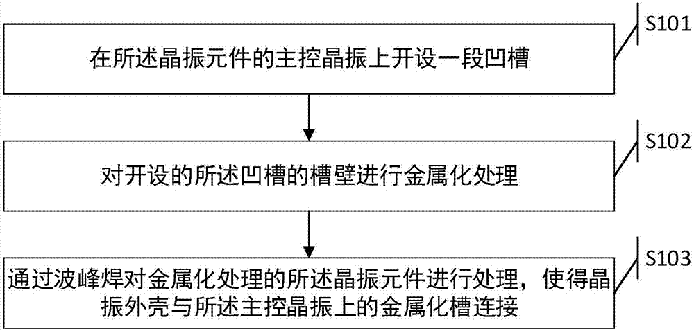
[0027] Such as figure 1 Shown is a flow chart of a method for manufacturing a crystal oscillator in an embodiment of the present invention, the method comprising:

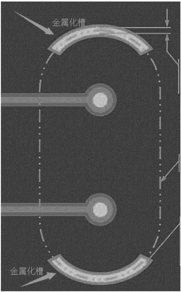
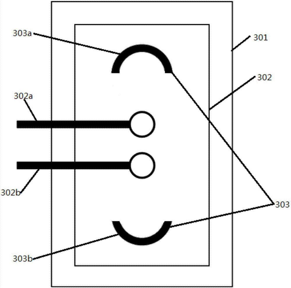
[0028] S101, creating a groove on the master crystal oscillator of the crystal oscillator element;

[0029] S102, performing metallization on the groove wall of the opened groove;

[0030] S103. Process the metallized crystal oscillator component by wave soldering, so that the crystal oscillator shell is connected to t...


PUM


Abstract

The invention discloses a manufacturing method of a crystal oscillator element and the crystal oscillator element. The method comprises the following steps: forming a segment of groove on a main control crystal oscillator of the crystal oscillator element, performing metallization processing on the groove wall of the formed groove, and processing the crystal oscillator element subjected to the metallization processing through wave soldering to connect a crystal oscillator housing with a metallized groove on the main control crystal oscillator. By adoption of the method, after a crystal oscillator material is inserted on a motherboard, the lower side of the main body of the crystal oscillator element has been in contact with the crystal oscillator package metallized groove on a PCB, then wave soldering is performed on the motherboard, so solder paste is automatically conveyed by the wave into the crystal oscillator package metallized groove, in this way, the crystal oscillator housing is connected with the metallized groove through the solder paste, and then the crystal oscillator housing is connected to the ground of the motherboard. Therefore, manual solder paste addition can be avoided, the quality of the product is improved, and the manufacturing cost is greatly reduced as well.

Description

technical field [0001] The present application relates to the field of communication technology, and in particular to a method for manufacturing a crystal oscillator component and the crystal oscillator component. Background technique [0002] Crystal oscillators for plug-ins are generally produced after manual plug-in in the dual inline-pinpackage (English: dual inline-pinpackage, DIP) section and then wave soldering. [0003] But for some machines that need certification, such as China or European countries, 3C or CE certification is required, but for some main control chips, their own power radiation is relatively large, causing the indicators to seriously exceed the standard. Tin treatment is added to the crystal oscillator, so that the crystal oscillator shell and the ground of the motherboard are connected together, reducing power radiation and space radiation. But at this time, another problem is brought about. The tinning of the shell of the crystal oscillator requi...

Claims


Application Information

Patent Timeline
Patent Type & Authority Applications(China)
IPC IPC(8): H03H3/02H03H9/05H03H9/10H03H9/17
Inventor 华学兵
Owner ZHUHAI GOTECH INTELLIGENT TECH
Features
  • Generate Ideas
  • Intellectual Property
  • Life Sciences
  • Materials
  • Tech Scout
  • Unparalleled Data Quality
  • Higher Quality Content
  • 60% Fewer Hallucinations
Learn More