Manufacturing method for semiconductor device

A manufacturing method and semiconductor technology, applied in semiconductor/solid-state device manufacturing, electrical components, circuits, etc., can solve problems such as yield loss, material loss, and difficulty in step height of shallow trench isolation structures, so as to improve performance and yield, The effect of small fluctuations in the height of the steps

Inactive Publication Date: 2017-06-30
SEMICON MFG INT (SHANGHAI) CORP +1
View PDF3 Cites 1 Cited by
  • Summary
  • Abstract
  • Description
  • Claims
  • Application Information

AI Technical Summary

Problems solved by technology

[0004] When the size of CMOS devices is reduced to the 28nm node and below, in the manufacturing process of the shallow trench isolation structure, after the hard mask layer SiN in the active region is removed, the step height of the shallow trench isolation structure (STI) (step high ) becomes increasingly difficult to control
Usually used in bench tools H 3 PO 4 to remove the

Method used


Image

  • Manufacturing method for semiconductor device
  • Manufacturing method for semiconductor device
  • Manufacturing method for semiconductor device

Examples


Example Embodiment

[0037] Example one

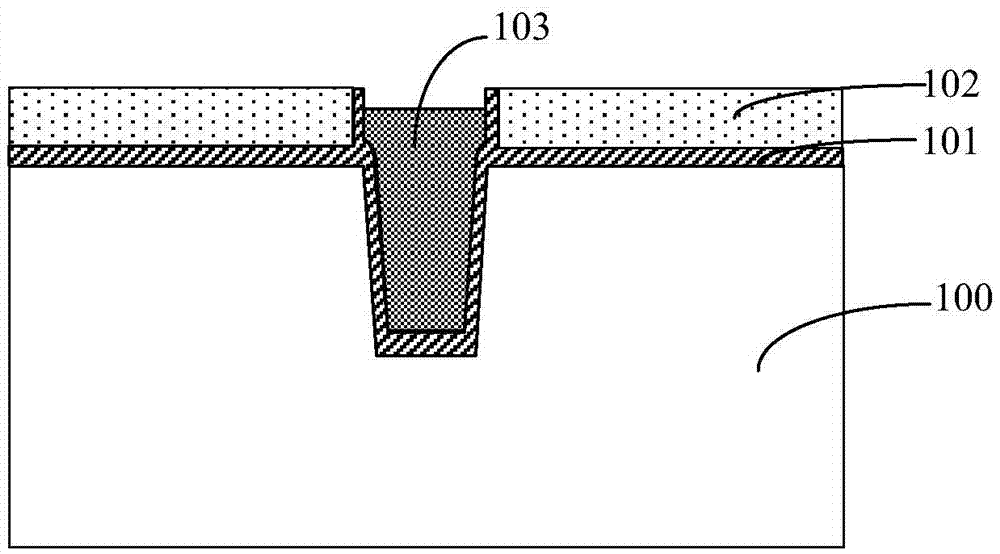
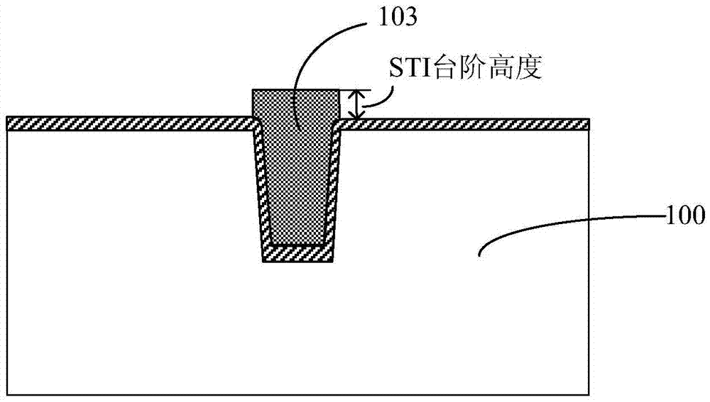
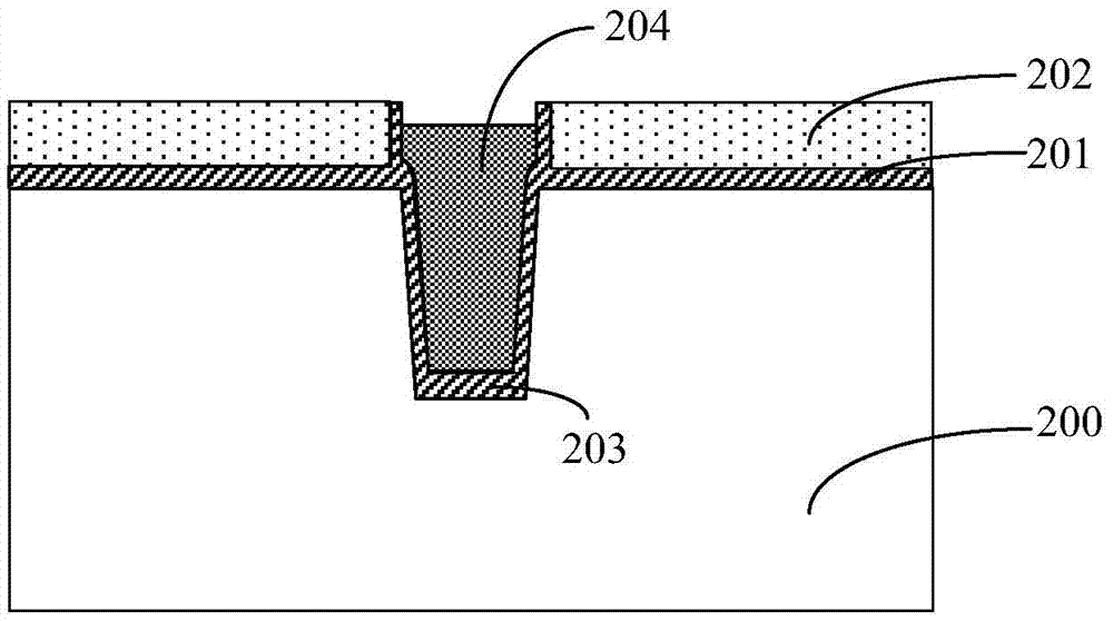
[0038] Below, refer to Figure 2A to Figure 2E as well as image 3 The detailed steps of an exemplary method of manufacturing a semiconductor device proposed by the embodiment of the present invention are described. Among them, 2A to Figure 2E Is a cross-sectional view of a structure formed in relevant steps of a method for manufacturing a semiconductor device according to an embodiment of the present invention; image 3 It is a schematic flowchart of a method for manufacturing a semiconductor device according to an embodiment of the present invention.

[0039] As an example, the method of manufacturing a semiconductor device of this embodiment specifically includes the following steps:

[0040] First, step S301 is performed to provide a semiconductor substrate, and a hard mask layer defining a pattern of a shallow trench isolation structure is formed on the surface of the semiconductor substrate.

[0041] Specifically, such as Figure 2A As shown, the constituen...


PUM


Abstract

The invention provides a manufacturing method for a semiconductor device, and relates to the technical field of semiconductors. The manufacturing method comprise providing a semiconductor substrate, and forming a hard mask layer defining the pattern of a shallow trench isolation structure on the surface of the semiconductor substrate; forming a shallow trench isolation structure in the semiconductor substrate with the surface of the shallow trench isolation structure being lower than that of the hard mask layer and higher than that of the semiconductor substrate; forming a protective layer on the surface of the shallow trench isolation structure through deposition; removing the hard mask layer; and removing the protective layer. According to the invention, by forming the protective layer on the shallow trench isolation structure, the surface of the shallow trench isolation structure can be effectively prevented from being etched and damaged during the wet method etching removal process of the hard mask layer, furthermore the STI step height fluctuation is small, and therefore the performance and the yield rate of the device are increased.

Description

technical field [0001] The invention relates to the technical field of semiconductors, in particular to a method for manufacturing a semiconductor device. Background technique [0002] In the semiconductor manufacturing process, the performance of the formed shallow trench isolation (STI) structure is critical to the performance and yield of the final formed semiconductor device. [0003] The manufacturing method of existing shallow trench isolation structure comprises the following main steps: as Figures 1A-1B As shown, at first, a buffer layer 101 and a hard mask layer (SiN) 102 are formed on a semiconductor substrate 100, the buffer layer and the hard mask layer are patterned, the semiconductor substrate is etched to form an opening of a shallow trench isolation structure, and then Deposit shallow trench isolation material 103 to fill the opening, and perform CMP to stop on the hard mask layer 102, and then remove the hard mask layer 102 to form a shallow trench isolatio...

Claims


Application Information

Patent Timeline
IPC IPC(8): H01L21/762
CPCH01L21/76232
Inventor 杨志勇
Owner SEMICON MFG INT (SHANGHAI) CORP
Why Eureka
Try Eureka