Assembling and manufacturing method for cell level liquid crystal of silicon-based liquid crystal

A technology of silicon-based liquid crystals and manufacturing methods, which is applied in the direction of instruments, nonlinear optics, optics, etc., can solve the problems of increased manufacturing costs, delayed development time, and increased time for liquid crystal alignment layers, reducing the required time and speeding up development time , Reduce the effect of process cycle time

Active Publication Date: 2017-07-04
SYNDIANT
View PDF9 Cites 3 Cited by
  • Summary
  • Abstract
  • Description
  • Claims
  • Application Information

AI Technical Summary

Problems solved by technology

[0005] However, the known technology fails to apply the same process or the same equipment in the manufacturing process of six-inch, eight-inch and twelve-inch wafers. When using the oblique evaporation method (SiO x / SiO 2 process) to form the liquid crystal alignment layer, the larger the size of the wafer, the larger the vacuum deposition system (vacuum deposition system), and thus increase the time to form the liquid crystal alignment layer; and when using the drop-in liquid crystal (ODF ), because the process state of each chip is not the same, the wafer process of larger size will be more complicated; moreover, the known technology must process the entire wafer, which cannot be processed as early as possible in the early stage of the manufacturing process. Screen out good bare chips and exclude inferior chips for follow-up procedures, resulting in a substantial increase in manufacturing costs; in addition, in the known technology, the bonding pad (bond pad) can only be located in the two last scribe and break areas ) on one of them; moreover, the process cycle time of the known technology is too long and thus delays the development time (development time); the circuit board of the liquid crystal display module (LCM) cannot be manufactured before the liquid crystal assembly process

Method used


Image

  • Assembling and manufacturing method for cell level liquid crystal of silicon-based liquid crystal
  • Assembling and manufacturing method for cell level liquid crystal of silicon-based liquid crystal
  • Assembling and manufacturing method for cell level liquid crystal of silicon-based liquid crystal

Examples


Embodiment Construction

[0035] The content of the present invention will be explained below through examples. However, the embodiments of the present invention are not intended to limit the present invention to be implemented in any environment, application or manner as described in the embodiments. Therefore, the descriptions about the embodiments are only for the purpose of illustrating the present invention, rather than directly limiting the present invention. It should be noted that in the following examples and illustrations, the steps that are not directly related to the present invention or those with ordinary knowledge in the field can understand how to implement them have been omitted and not shown. And those skilled in the art should understand that the liquid crystal assembly method disclosed in the present invention can be applied to various occasions.

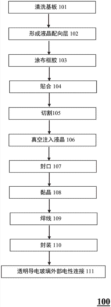
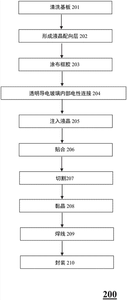
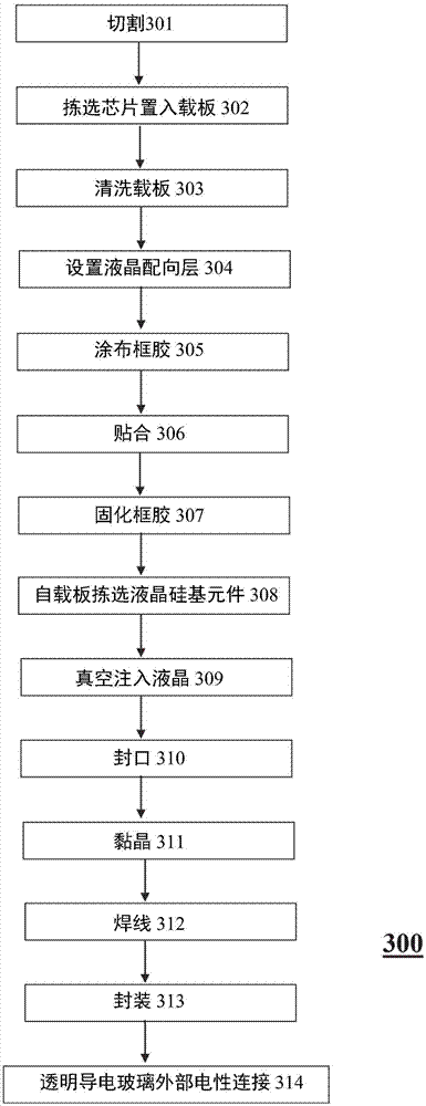
[0036] Please see image 3 , which is a flow chart of one embodiment of the cell-level liquid crystal assembly and manufacturing metho...


PUM


Abstract

The invention relates to an assembling and manufacturing method for cell level liquid crystal of silicon-based liquid crystal. The method comprises: cutting silicon wafers and a transparent conducting glass substrate and performing cell singulation, choosing proper cut silicon dies and transparent conducting glass chips to respectively put the cut dies and transparent conducting glass chips in different carrier plates, cleaning the carrier plates, respectively forming a liquid crystal orientation layer on the carrier plate, and then performing two subsequent steps: in a first method, after coating a frame adhesive, adhering the silicon dies and transparent conducting glass chips and then curing the frame adhesive, and then choosing a proper liquid crystal silicon-based cell from the carrier plates, injecting the liquid crystal silicon-based cell into liquid crystal in a vacuum manner and sealing, then performing die bond and bonding wire and then packaging, finally, the external part being electrically connected with the transparent conducting glass; or in a second method, after coating a frame adhesive, the internal part being electrically connected with the transparent conducting glass, after one drop fill (ODF), adhering the silicon dies and transparent conducting glass chips, and finally, curing the frame adhesive, and performing die bond, bonding wire, and packaging.

Description

[0001] 【Technical field】 [0002] The invention relates to a liquid crystal assembly and manufacturing method, in particular to a silicon-based liquid crystal unit-level liquid crystal assembly and manufacturing method. [0003] 【Background technique】 [0004] figure 1 It is a flow chart of a liquid crystal assembly and manufacturing method for external electrical connection with transparent conductive glass (ITO) and vacuum injection of liquid crystal in the known technology. Such as figure 1 As shown, the liquid crystal assembly and manufacturing method in the known technology is to first clean the substrate 101 , form a liquid crystal alignment layer 102 , and then apply a sealant 103 and stick them together 104 . Then silicon wafer and transparent conductive glass substrate are cut and separated (cell singulation) 105 , liquid crystal 106 is vacuum injected and then sealed 107 , followed by die bonding 108 , wire bonding 109 and packaging 110 , and finally external electr...

Claims


Application Information

Patent Timeline
Patent Type & Authority Applications(China)
IPC IPC(8): G02F1/13
CPCG02F1/1303
Inventor 黄振潮王协友
Owner SYNDIANT
Why Eureka
Try Eureka