Efficient silicon wafer printing machine

A technology for printing presses and silicon wafers, applied in printing presses, rotary printing presses, screen printing presses, etc., can solve the problems of low positioning efficiency, low production efficiency, and insufficient printing effect, and achieve rapid positioning and improve efficiency. Effect

Pending Publication Date: 2017-07-07
EGING PHOTOVOLTAIC TECHNOLOGY CO LTD
7 Cites 2 Cited by

AI-Extracted Technical Summary

Problems solved by technology

[0004] The technical problem to be solved by the present invention is: in order to solve the existing photovoltaic solar high-efficiency silicon wafer printing machine, the positioning of the silicon wafer is not accurate...

Abstract

The invention relates to the technical field of silicon wafer production equipment, in particular to an efficient silicon wafer printing machine. The efficient silicon wafer printing machine comprises a rack and a workbench rotationally arranged on the rack. A conveying belt used for conveying silicon wafers is arranged on the workbench. An adjusting plate is rotationally arranged on the workbench and corresponds to the conveying belt. An air cylinder used for driving the adjusting plate to rotate is arranged on the rack. The stretching-out end of the air cylinder is in threaded connection with an adjusting nut. An ejector rod is rotationally arranged on the adjusting nut. When the efficient silicon wafer printing machine is used, the adjusting nut is controlled, the contact distance between the ejector rod and the adjusting plate can be adjusted, and therefore the rotating angle of the adjusting plate is changed so as to achieve silicon wafer fast locating, and the silicon wafer locating efficiency is improved; and the problems that in an existing photovoltaic solar efficient silicon wafer printing machine, silicon wafer locating is inaccurate, the locating efficiency is low, the printing effect is not good enough, the printing precision is not high enough, and the production efficiency is low are solved.

Application Domain

Screen printers

Technology Topic

PhysicsSilicon chip +4

Image

  • Efficient silicon wafer printing machine
  • Efficient silicon wafer printing machine
  • Efficient silicon wafer printing machine

Examples

  • Experimental program(1)

Example Embodiment

[0019] Example
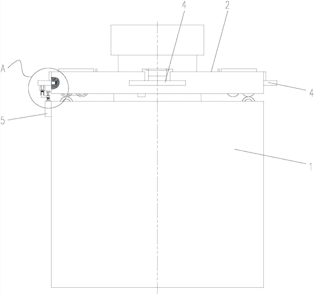
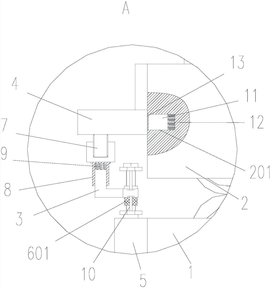
[0020] like Figure 1-3 As shown, a high-efficiency silicon wafer printing machine includes a frame 1 and a workbench 2 rotatably arranged on the frame 1. The workbench 2 is provided with a conveyor belt for conveying silicon wafers, and the conveyor belt passes through the frame. The friction wheel on 1 is driven to rotate, and an adjustment plate 4 is installed on the workbench 2. The adjustment plate 4 corresponds to the conveyor belt, and the frame 1 is provided with a cylinder for driving the adjustment plate 4 to rotate. 5. An adjusting nut 6 is threadedly connected to the protruding end of the cylinder 5, and a push rod 3 is rotated on the adjusting nut 6, and the push rod 3 is in contact with the adjusting plate 4.
[0021] The push rod 3 is provided with a roller 7 , and the roller 7 is in contact with the regulating plate 4 .
[0022] The roller 7 is provided with a sliding sleeve 8 , the sliding sleeve 8 is sleeved on the push rod 3 , and a first spring 9 is provided between the sliding sleeve 8 and the push rod 3 .
[0023] A guide shaft 10 is provided on the protruding end of the cylinder 5 , and the push rod 3 is slidably disposed on the guide shaft 10 .
[0024] The adjusting nut 6 is provided with a knurling 601 .
[0025] The workbench 2 is provided with a chute 201, a buffer block 11 is slidably arranged in the chute 201, a second spring 12 is arranged between the chute 201 block and the chute 201, and the buffer block 11 is in contact with the regulating plate 4 .
[0026] Protruding points 13 are provided on the contact surface between the buffer block 11 and the adjusting plate 4, and the material of the protruding points 13 is rubber.
[0027] When the above-mentioned high-efficiency silicon wafer printing machine is adjusted, the specific operation steps are as follows: firstly control the adjustment nut 6, the adjustment nut 6 rotates on the ejector rod 3, and drives the ejector rod 3 to move on the extension end of the cylinder 5, and the ejector rod 3 guides Displacement on the shaft 10 can be done by adjusting the distance between the roller 7 on the push rod 3 and the adjustment plate 4 as required, and the adjustment of the distance between the roller 7 and the adjustment plate 4 is completed. When in use, start the cylinder 5, the extended end of the cylinder 5 drives the push rod 3 to rise, and the push rod 3 drives the roller 7 at the same time, and makes the roller 7 approach the adjustment plate 4; when the roller 7 contacts the adjustment plate 4, the roller 7 goes up The first spring 9 between the sliding sleeve 8 and the push rod 3 is squeezed, eliminating the impact force between the roller 7 and the adjustment plate 4, and the roller 7 lifts the adjustment plate 4, so that the adjustment plate 4 is on the workbench 2 Rotate upwards, so that the silicon wafer follows the rotation and tilts to one side for positioning. After the positioning of the silicon wafer is completed, the cylinder 5 is controlled to shrink. Plate 4 can be restored to its original state. When the cylinder 5 fails, the adjustment plate 4 rotates quickly and returns to its original shape. At the same time, the adjustment plate 4 is in contact with the buffer block 11. On the one hand, the bump 13 is used for buffering and damping between the adjustment plate 4 and the buffer block 11, and then the working table 2 The second spring 12 in the upper chute 201 buffers and damps the adjustment plate 4 to prevent the collision between the adjustment plate 4 and the workbench 2. There are several buffer blocks 11 evenly along the circumference.

PUM

no PUM

Description & Claims & Application Information

We can also present the details of the Description, Claims and Application information to help users get a comprehensive understanding of the technical details of the patent, such as background art, summary of invention, brief description of drawings, description of embodiments, and other original content. On the other hand, users can also determine the specific scope of protection of the technology through the list of claims; as well as understand the changes in the life cycle of the technology with the presentation of the patent timeline. Login to view more.

Similar technology patents

Method and system for positioning playing of online video

ActiveCN105578262ARapid positioningShorten positioning waiting time
Owner:TCL CORPORATION

Address quick positioning method and device, computer equipment and storage medium

PendingCN111611290ARapid positioningImprove address location efficiency
Owner:广东中科慧据科技有限公司

Synchronization triggering on-line diagnostic method and system for photoetching machine

ActiveCN101359187BRapid positioningSave time on integration and technical support
Owner:SHANGHAI MICRO ELECTRONICS EQUIP (GRP) CO LTD

Cross-shaped four-aperture field-of-view partially-overlapped bionic thermal imaging system

ActiveCN110595624AAlleviate the contradiction between field of view and resolutionRapid positioning
Owner:BEIJING INSTITUTE OF TECHNOLOGYGY

Classification and recommendation of technical efficacy words

  • Rapid positioning
  • Improve efficiency

Remote-sensing data management system and method

ActiveCN102662610ARapid positioningReduce search pressure
Owner:AEROSPACE INFORMATION RES INST CAS

Unilateral positioning method for secondary docking of ship in dock

Owner:CSSC HUANGPU WENCHONG SHIPBUILDING COMPANY
Why Eureka
Try Eureka