

Photomask particle size assessment method
A particle size and photomask technology, applied in optics, optomechanical equipment, microlithography exposure equipment, etc., can solve problems such as tight specifications, product misflow, rework, etc., and achieve the effect of reducing unnecessary rework and increasing costs
- Summary
- Abstract
- Description
- Claims
- Application Information
AI Technical Summary
Problems solved by technology
Method used
Image

Examples
Embodiment Construction
[0031] The specific embodiment of the present invention will be further described in detail below in conjunction with the accompanying drawings.
[0032] It should be noted that in the following specific embodiments, when describing the embodiments of the present invention in detail, in order to clearly show the present invention for the convenience of description, the structures in the drawings are not drawn according to the general scale, and partial Enlargement, deformation and simplified processing, therefore, should be avoided as limiting the understanding of the present invention.
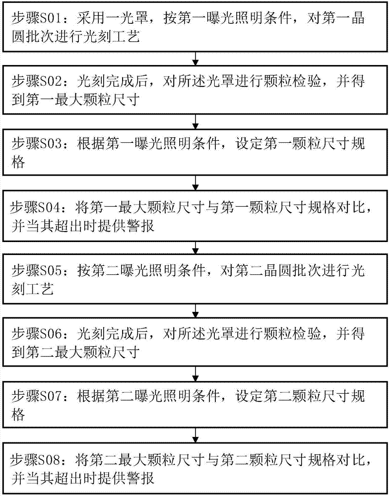
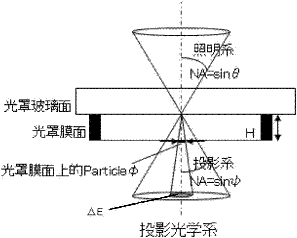
[0033] In the following specific embodiments of the present invention, first please refer to figure 2 , figure 2 It is a schematic diagram of the application of the projection optical system on the mask. Such as figure 2 As shown in FIG. 1 , it shows a commonly used glass mask with a photolithographic pattern film surface formed on the surface. During the photolithography process, part...
PUM
 Abstract
Description
Claims
Application Information