Embedded system

A system bus and data writing technology, applied in the computer field, can solve problems such as program data storage security, and achieve the effect of safe storage and protection from being stolen

Pending Publication Date: 2017-07-07
GIGADEVICE SEMICON (BEIJING) INC
View PDF5 Cites 3 Cited by
  • Summary
  • Abstract
  • Description
  • Claims
  • Application Information

AI Technical Summary

Problems solved by technology

[0006] The invention provides an embedded system to solve the security problem of program data storage

Method used


Image

  • Embedded system
  • Embedded system
  • Embedded system

Examples


Embodiment 1

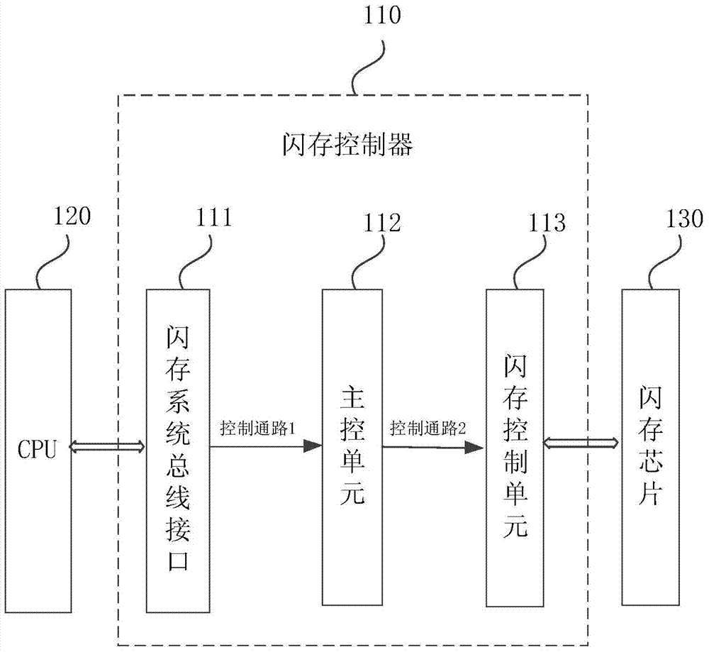
[0042] figure 1 A schematic structural diagram of an embedded system provided by Embodiment 1 of the present invention, such as figure 1 As shown, the embedded system provided by this embodiment includes: a flash memory controller 110, a central processing unit (CPU) 120 and a flash memory chip 130, and the flash memory controller 110 is connected to the CPU 120 and the flash memory chip 130 respectively, wherein the CPU 120 It is used to control the operation of the flash memory controller 110 and the flash memory chip 130; the flash memory chip 130 is readable and rewritable, and the stored data information will not be lost when the power is turned off.

[0043]The flash memory controller 110 is configured on the main chip of the embedded system, and the main chip and the flash memory chip can be manufactured in the same package by using MCP (Multiple Chip Package) technology to form an embedded system.

[0044] The flash memory controller 110 is used for exchanging state i...

Embodiment 2

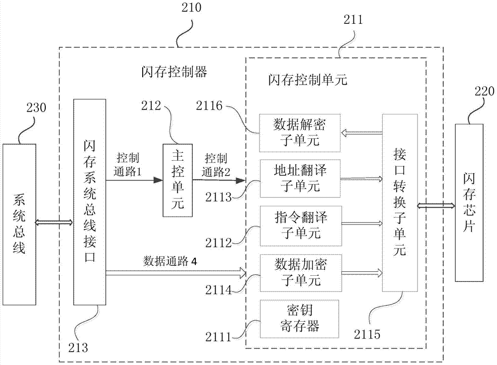
[0052] figure 2 A schematic structural diagram of an embedded system provided in Embodiment 2 of the present invention, such as figure 2 As shown, this embodiment provides a preferred implementation solution of the flash memory controller 210 on the basis of the foregoing embodiments.

[0053] The flash memory control unit 211 includes: a key register 2111 , an instruction translation subunit 2112 , an address translation subunit 2113 , a data encryption subunit 2114 , an interface conversion subunit 2115 and a data decryption subunit 2116 .

[0054] The key register 2111 is used to store the encryption key and the decryption key.

[0055] The key register 2111 is connected with the flash memory chip 220, and is used for automatically reading the encryption key and the decryption key from the flash memory chip 220 after the system is powered on, and storing them. Further, the encryption key and the decryption key stored in the key register 2111 may be pre-configured. The ...

Embodiment 3

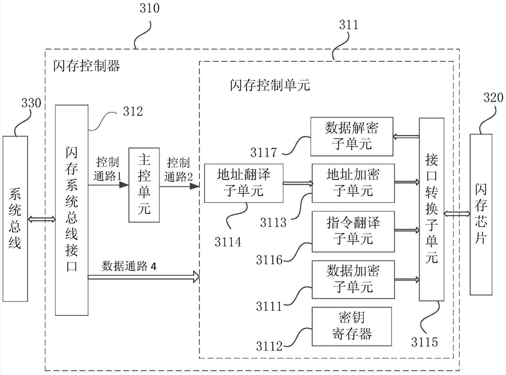
[0067] image 3 A schematic structural diagram of a flash memory control unit provided in Embodiment 3 of the present invention, as shown in image 3 As shown, this embodiment provides a preferred implementation solution of an encryption key on the basis of the foregoing embodiments.

[0068] The encryption key may include: an address encryption key and a data encryption key;

[0069] The data encryption subunit 3111 is specifically configured to receive the program data sent by the flash memory system bus interface 312, obtain the data encryption key stored in the key register 3112, and use the data encryption key to encrypt the received program data. The program data is encrypted to obtain the ciphertext of the program data.

[0070] The flash memory control unit 311 preferably also includes:

[0071] The address encryption subunit 3113 is respectively connected to the address translation subunit 3114, the key register 3112 and the interface conversion subunit 3115, and i...


PUM


Abstract

The present invention discloses an embedded system. The embedded system comprises a flash memory controller, a CPU and a flash memory chip. The flash memory controller is respectively connected with the CPU and the flash memory chip, and the flash memory controller comprises a flash memory system bus interface; a main control unit, which is connected with the flash memory system bus interface; and a flash memory control unit, which is respectively connected with the flash memory system bus interface, the main control unit and the flash memory chip, is used for encrypting program data corresponding to a data write instruction to obtain the program data ciphertext and writing the program data ciphertext to the flash memory chip according to the received data write instruction and the corresponding address, and is further used for, according to the received data write instruction and the corresponding address, reading the program data ciphertext stored in the flash memory chip, decrypting the program data ciphertext to obtain the corresponding program data, and providing the program data for the CPU to execute. According to the technical scheme of the present invention, the program data can be effectively protected from being stolen, so that safe storage of the program data can be realized fundamentally.

Description

technical field [0001] The embodiments of the present invention relate to the technical field of computers, and in particular to an embedded system. Background technique [0002] Microcontrollers (Micro Control Unit, MCU) are widely used, ranging from small children's toys to large construction machinery. When the MCU chip is applied, the user needs to spend a lot of manpower and material resources on software development, and the final program data is stored in the flash memory, and these program data belong to the user's intellectual property rights and should be prevented from being stolen by other users. Illegal intruders may use violence to disassemble the chip and forcibly read out the data in the flash memory. [0003] MCU chips usually store program data directly into flash chips. At present, in order to ensure the security of the program data, the existing technology usually adopts the flash memory chip embedded in the MCU chip during the production of the MCU chi...

Claims


Application Information

Patent Timeline
Patent Type & Authority Applications(China)
IPC IPC(8): G06F21/79
CPCG06F21/79
Inventor 王南飞
Owner GIGADEVICE SEMICON (BEIJING) INC
Why Eureka
Try Eureka