Packaging structure of image sensor

An image sensor and packaging structure technology, applied in the direction of electric solid-state devices, semiconductor devices, radiation control devices, etc., can solve problems such as shooting quality interference, achieve the effects of suppressing reflection, reducing interfering light, and improving imaging quality

Inactive Publication Date: 2017-07-07
BEIJING UNIV OF TECH
View PDF4 Cites 10 Cited by
  • Summary
  • Abstract
  • Description
  • Claims
  • Application Information

AI Technical Summary

Problems solved by technology

[0003] However, the current packaging solutions are mainly aimed at image sensors with low and medium pixels. With the improvement of pixels and shooting quality requirements, the impact of the above-mentioned packaging solutions on the light incident on the photosensitive area must be minimized by the external pollution of the glass. The reflection on the structural parts also needs to be strictly controlled. The interference of glare, ghosting and other phenomena on the shooting quality cannot be ignored

Method used


Image

  • Packaging structure of image sensor

Examples


Embodiment Construction

[0014] In order to make the technical solution of the present invention more comprehensible, the specific implementation manners of the present invention will be described in detail below in conjunction with the accompanying drawings. For convenience of description, the components in the structures in the drawings of the embodiments are not scaled according to the normal scale, so they do not represent the actual relative sizes of the structures in the embodiments. The above or upper side of the structure or surface includes the case where there are other layers in the middle.

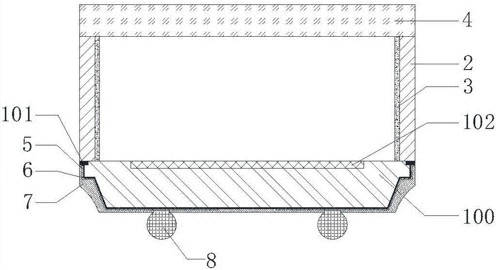
[0015] Examples of the present invention figure 1 As shown, an image sensor packaging structure includes an image sensor chip 100 with at least one photosensitive area 102 and a plurality of welding pads 101 on the functional surface, and a cofferdam 2 is bonded on the functional surface, and the bottom surface of the cofferdam 2 covers On the surface of the chip on the periphery of the photosensitive...


PUM


Abstract

The invention discloses a packaging structure of an image sensor. A light-absorbing layer is covered on an inner sidewall. Meanwhile, a cofferdam higher than 100 mum is adopted instead of a relatively low photoresist polymer cofferdam, so that the distance between contamination particles on the surface of a light-transmitting cover plate and a photosensitive region is increased. The affected area of the light blocked by the particles in the photosensitive region is reduced, and the incidence angle of the incident light is also reduced. The light-absorbing layer is covered on the inner sidewall of the cofferdam, so that the reflection of the obliquely incident light or the reflected light in the photosensitive region on the inner sidewall of the cofferdam is effectively inhibited. The interference light shooting into the photosensitive region is reduced, and the imaging quality is improved.

Description

technical field [0001] The invention relates to wafer-level packaging of semiconductor chips, in particular to an image sensor packaging structure. Background technique [0002] The current mainstream of the wafer-level packaging solution for image sensors is to bond the ordinary glass cover and its photoresist polymer cofferdams below 70 μm on the surface to the functional surface of the wafer of the image sensor. Each cofferdam corresponds to each image. The sensor chip makes the position of the photosensitive area form a sealed cavity. Perform TSV process on the non-functional surface of the wafer, and make metal lines to lead the pads on the functional surface to the non-functional surface of the wafer through the TSV opening. After making bumps on the non-functional surface, it is cut to form a single chip. [0003] However, the current packaging solutions are mainly aimed at image sensors with low and medium pixels. With the improvement of pixels and shooting quality...

Claims


Application Information

Patent Timeline
Patent Type & Authority Applications(China)
IPC IPC(8): H01L27/146
CPCH01L27/14618H01L27/14623H01L27/14625
Inventor 秦飞唐涛别晓锐项敏肖智轶
Owner BEIJING UNIV OF TECH
Why Eureka
Try Eureka