Input-parallel output-series wide-gain boost-type direct-current converter used for fuel cell
A technology of DC converter and output series connection, which is applied in the direction of battery/fuel cell control device, output power conversion device, converter type, etc., and can solve small input current ripple, increased switching loss, large input current ripple, etc. problem, to achieve the effect of wide voltage gain, prolong service life, and reduce input current ripple
- Summary
- Abstract
- Description
- Claims
- Application Information
AI Technical Summary
Problems solved by technology
Method used
Image
Examples
Embodiment 1
[0028] (1) Topology
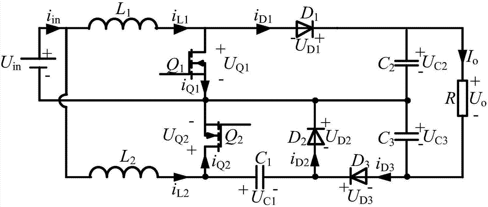
[0029] The embodiment of the present invention proposes as figure 1 The shown input parallel-output series wide-gain boost DC converter topology. Inductance L 1 , the power switch Q 1 , Diode D 1 and capacitance C 2 Constitute the traditional boost DC converter topology, the inductor L 2 , the power switch Q 2 , Diode D 2 and D 3 , capacitance C 1 and C 3 A boost DC converter topology in which the output voltage is reversed to the input voltage is formed. The two are connected in parallel with the input and connected in series to form a wide-gain input parallel and output series boost DC converter topology. The power input terminal of the DC converter is connected with the fuel cell (using U in Indicated) is connected; the output terminal is connected with the high-voltage DC bus (indicated by load R).
[0030] (2) Wide voltage gain
[0031] The topology proposed in the embodiment of the present invention adopts an interleaved parallel contro...
Embodiment 2
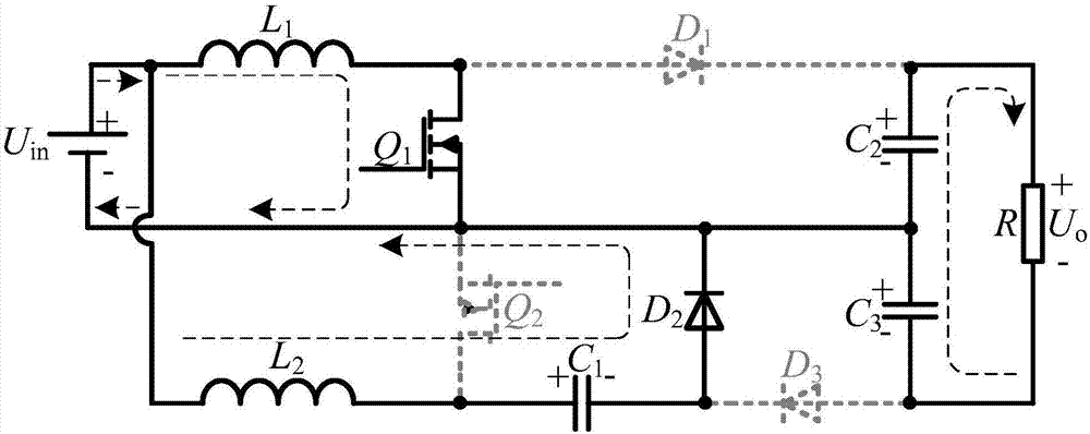
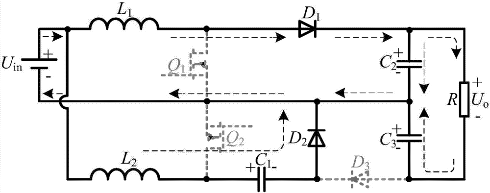
[0050] Below to figure 1 The novel input parallel-output series wide-gain boost DC converter topology shown, figure 2 , 3 , the topological energy flow path diagram shown in 4 and 5, and Figure 6 , 7 The important working waveforms of the new topology are shown, and the principle of the DC converter is further introduced. See the description below for details:
[0051] Switching state 10: Power switch Q 1 conduction, Q 2 off, the diode D 1 and D 3 off, D 2 conduction, at this time the inductor current i L1 increases linearly, i L2 linearly decreases, the inductor current i L2 For capacitance C 1 charge, capacitor C 2 and C 3 discharge, the load energy is supplied by the capacitor C 2 and C 3 supply.
[0052] Switch state 00: power switch Q 1 and Q 2 off, the diode D 1 and D 2 conduction, D 3 turn off, at this time the inductor current i L1 and i L2 linearly decreases, the inductor current i L2 For capacitance C 1 charge, capacitor C 3 discharge, the...
PUM
 Abstract
Description
Claims
Application Information


