Isolator and isolator manufacturing method

a manufacturing method and isolation technology, applied in the direction of fixed transformers or mutual inductances, semiconductor/solid-state device details, analog circuits affected by digital noise, etc., can solve the problems of inability to manufacture photocouplers on semiconductor substrates by general integrated circuit (ic) process, integrated with transmission circuits, etc., to reduce the dc resistance of the primary coil, reduce the cross-sectional area of the primary coil, reduce the effect of coil-induced magnetic effects on the transmission circui

Active Publication Date: 2013-12-05
FUJI ELECTRIC CO LTD
View PDF3 Cites 29 Cited by
  • Summary
  • Abstract
  • Description
  • Claims
  • Application Information

AI Technical Summary

Benefits of technology

[0031]In some embodiments, a transmission circuit can be disposed in a first principal surface of a semiconductor substrate and a transformer configured by a primary coil and a secondary coil can be disposed in an entire second principal surface of the semiconductor substrate. As a result, even if a transmission circuit and a transformer are disposed in a single semiconductor substrate, the semiconductor substrate can be reduced in size to a degree just fitting the outer most peripheries of the coils configuring the transformer.
[0032]In some embodiments, by disposing the transformer in the second principal surface of the semiconductor substrate, a signal from the transmission circuit disposed in the first principal surface of the semiconductor substrate can be extracted from the second principal surface side of the semiconductor substrate. Consequently, the coil-induced magnetic effects on the transmission circuit disposed in the first principal surface of the semiconductor substrate can be reduced. Further, the integration of the transmission circuit and the reception circuit in different semiconductor substrates enables the occurrence of transmission circuit malfunctions consequent to dV / dt occurring at the reception circuit side to be suppressed. Moreover, since the transformer does not require magnetic bodies among the components, the transformer is not limited to the characteristics of operating frequency by the hysteresis of magnetic bodies.
[0033]In some embodiments, the primary coil is configured by a metal film embedding the trench, thereby enabling the cross-sectional area of the primary coil to be increased according to the depth of the coil trench. Consequently, the DC resistance of the primary coil can be decreased and a large voltage gain can be obtained. Further the primary coil is formed within the trench and the secondary coil is formed within the insulating film and consequently, the coils do not oppose one another at trench side walls, like a conventional transformer having coils formed in 2 trenches, respectively. Therefore, compared to a conventional transformer, the area of the portion where the primary coil and the secondary coil opposed one another can be reduced. Accordingly, parasitic capacitance between the primary coil and the secondary coil can be reduced, thereby enabling the delay of signal transmission from the transmission circuit to the reception circuit to be reduced. Accordingly, the electrical characteristics of the isolator can be improved. Further, the thickness of the insulating film at the portion sandwiched by the primary coil and the secondary coil can be easily increased, thereby enabling high voltage tolerance to be facilitated.

Problems solved by technology

For example, when an analog circuit and a digital circuit are connected at a common reference potential, the analog circuit is affected by digital noise.
On the other hand, photocouplers cannot be fabricated (manufactured) on a semiconductor substrate by a general integrated circuit (IC) process.
Consequently, photocouplers cannot be integrated with transmission circuits nor with reception circuits and are disposed as a separate component in a signal processor, making size reductions of signal processors difficult.
Further, the luminous efficiency of photodiodes temporally degrades consequent to operating conditions such as operating temperature and forward current.
In addition, the photocoupler has a slow response speed requiring periods on the order of microseconds for signal transmission.
As a result, for example, an inverter drive circuit equipped with a photocoupler has to establish dead time on the order of microseconds for the device configured by the inverter and thus, increases in speed are not possible.
Nonetheless, coupling capacitors have a problem of being easily affected by noise and external electric fields.
However, despite having high insulation resistance and high resistance to noise, these transformers further have a high cost and high power consumption.
Furthermore, since the coils in the transformers are large, a reduction in the size of the transformer is difficult.
Like photocouplers, the coupling capacitors and the transformers are also equipped in signal processors as a separate component, making a reduction in the size of the signal processor difficult.
Thus, with respect to a signal processor equipped with a photocoupler, a coupling capacitor, or a transformer, a problem arises in that reductions in the size of the signal processor become difficult.
However, since the HVIC cannot perform isolated transmission of signals, tolerability of high voltages is difficult to facilitate, e.g., a voltage tolerance of a mere 1200V can be guaranteed.
Further, since the HVIC has a low tolerance to noise and is easily damaged, the HVIC is not applicable to devices for which reliability is required.
However, the isolators of Non-Patent Literature 1 and 2 have cylindrical-shaped coils (solenoid coils) of spirally wound metal wire and because the thickness of the metal wire forming the coil cannot be increased, problems of increased DC resistance of the coil and decreased voltage gain arise.
Furthermore, since overcurrent arises and the coil generates heat, a problem of large loss arises.
Consequently, problems arise in that the DC resistance of the coil is high and the voltage gain is small.
Therefore, a problem arises in that high voltage tolerance becomes difficult.
As a result, large parasitic capacitance arises and the isolator is easily affected by noise.

Method used


Image

  • Isolator and isolator manufacturing method
  • Isolator and isolator manufacturing method
  • Isolator and isolator manufacturing method

Examples


first embodiment

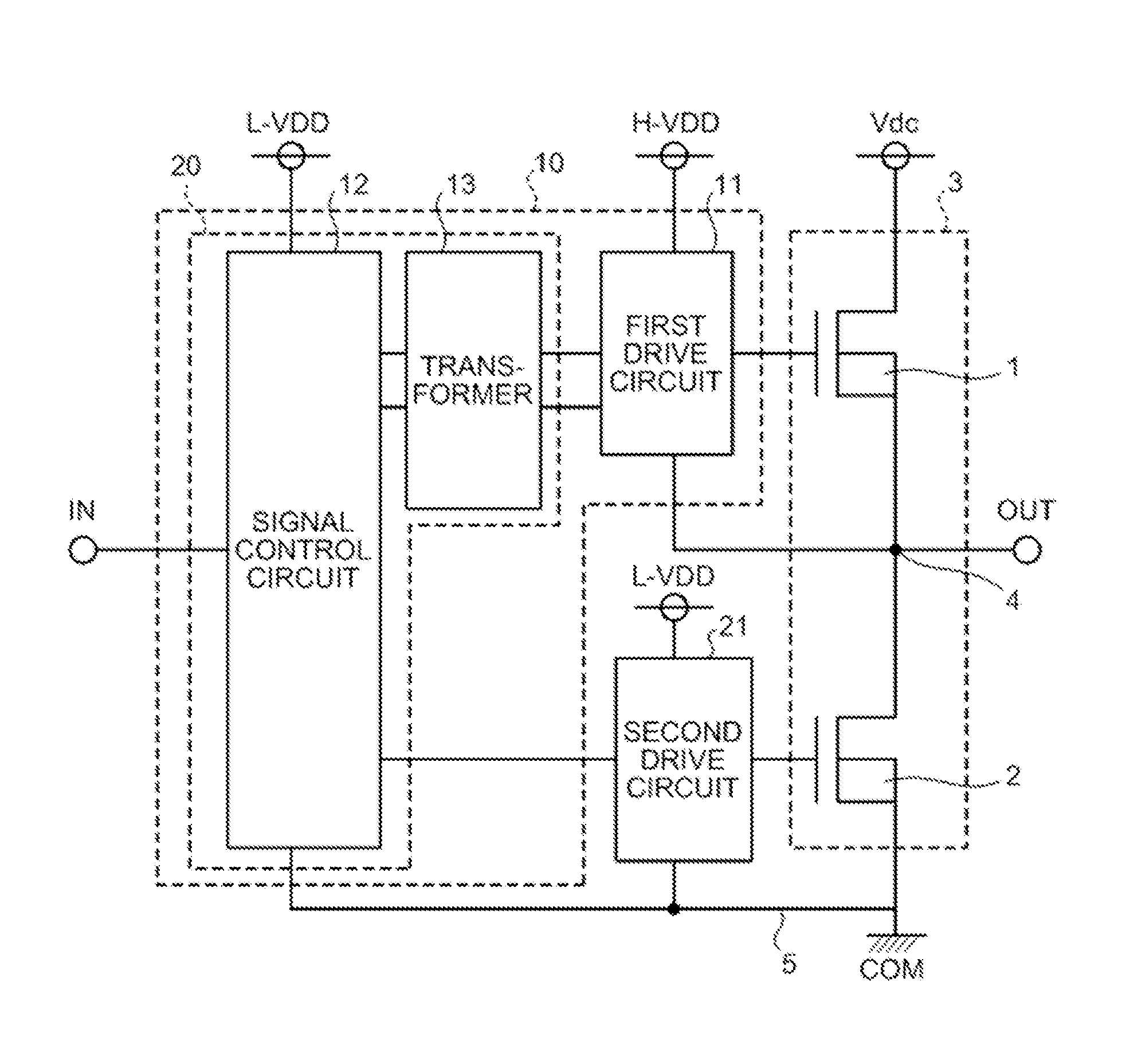
[0054]FIG. 1 is a block diagram depicting an example of an overall configuration of a semiconductor device to which an isolator according to a first embodiment is applied. An example of an overall configuration of a semiconductor device to which the isolator according to the present invention is applied will be described. The semiconductor device depicted in FIG. 1 is configured by a bridge circuit 3 configured by a first metal-oxide-semiconductor field effect transistor (MOSFET) 1 and a second MOSFET 2; an isolator 10 that includes a first drive circuit 11 that drives the first MOSFET 1 of the upper arm; and a second drive circuit 21 that drives the second MOSFET 2 of the lower arm.

[0055]The bridge circuit 3 is an external-output circuit that via a connection point 4 of the source of the first MOSFET 1 and the drain of the second MOSFET 2, outputs a signal from an output terminal OUT to an external destination. The drain of the first MOSFET 1 of the upper arm is connected to source...

second embodiment

[0091]FIG. 15 is a schematic cross sectional view of the isolator according to a second embodiment. The isolator 100 according to the second embodiment differs from the isolator according to the first embodiment in that the bump electrodes 32-2 of the transformer mounted chip 20 are directly connected to the terminals 51 of the reception circuit 11 of the signal reception chip 50. In other words, in the second embodiment, the connection of the secondary coil 32-1 disposed on the transformer mounted chip 20 and the reception circuit 11 disposed on the signal reception chip 50 does not use bonding wire.

[0092]The signal reception chip 50 is joined to an anterior surface of a mounting substrate 70 formed by the insulating substrate, a posterior surface thereof being regarded as the mounting substrate 70 side. The transformer mounted chip 20, with the posterior surface being regarded as the signal reception chip 50 side, is placed on the anterior surface of the signal reception chip 50. ...

third embodiment

[0094]FIG. 16 is a block diagram of an example of an overall configuration of a semiconductor device to which the isolator according to a third embodiment is applied. An isolator 110 according to the third embodiment differs from the isolator according to the first embodiment on the following 2 points. The first difference is that in the basic circuit unit of the signal control circuit (hereinafter, first signal control circuit) 121, not just the transmission circuit, but also a reception circuit that receives a signal from another signal control circuit (hereinafter, second signal control circuit) 122 is configured therein. The second difference is that in place of the first drive circuit, the second signal control circuit 122 and a second transformer 123 are further included, and an upward level-shifting function and a downward level-shifting function are implemented by 2 transformers, the first and the second transformers 13, 123, disposed in the isolator 110.

[0095]As depicted in...


PUM


Abstract

In certain aspects of the invention, an isolator is configured by a reception circuit, a transmission circuit, and a transformer. In some aspects, the transmission circuit is disposed in an anterior surface of a semiconductor substrate. The transformer is disposed in a posterior surface of the semiconductor substrate and transmits in an electrically isolated state to the reception circuit, a signal input from the transmission circuit. The transformer is configured by a primary coil and a secondary coil. The primary coil can be configured by a metal film embedded in an oxide film inside a coil trench. The secondary coil can be disposed inside an insulating film covering the primary coil so as to oppose the primary coil and is insulated from the primary coil by the insulating film.

Description

CROSS-REFERENCE TO RELATED APPLICATION[0001]This application is a continuation of International Application No. PCT / JP2012 / 003512, filed on May 29, 2012. The disclosure of the PCT application, in its entirety, including the drawings, claims, and the specification thereof, is incorporated herein by reference.BACKGROUND[0002]1. Field of the Invention[0003]The present invention relates to an isolator and isolator manufacturing method.[0004]2. Background Related Art[0005]Various types of apparatuses, such as devices used for industrial or medical purposes, often require electrical insulation. For example, an electronic device controlled by high voltage is equipped with a signal isolator (isolator) so that when a signal received by the electronic device is transmitted to an external device or when the user directly manipulates the operation panel, the user is not subjected to electrical shock or other severe bodily harm. When the electrical potential difference between electronic devices...

Claims


Application Information

Patent Timeline
Patent Type & Authority Applications(United States)
IPC IPC(8): H01P1/36H01L21/768
CPCH01L23/481H01L21/76879H01L2924/13091H01L2224/73257H01L2225/06531H01P1/36H01F2019/085H01L23/5227H01L23/645H01L24/16H01L25/0652H01L25/0657H01L28/10H01L2224/13022H01L2224/16238H01L2924/00014H01L2225/06513H01L2225/06541H01L2224/13099H01L2924/00H01L2924/12043
Inventor SUMIDA, HITOSHITOYODA, YOSHIAKIAKAHANE, MASASHI
Owner FUJI ELECTRIC CO LTD
Why Eureka
Try Eureka