Bandgap reference circuit and method for producing the circuit

a reference circuit and bandgap technology, applied in the direction of electric variable regulation, process and machine control, instruments, etc., can solve the problem of reducing the sensitivity to supply voltage variations, and achieve the effect of low minimum required supply voltage, low current consumption, and small chip area

Active Publication Date: 2012-11-06
SNAPTRACK
View PDF8 Cites 5 Cited by
  • Summary
  • Abstract
  • Description
  • Claims
  • Application Information

AI Technical Summary

Benefits of technology

[0004]It is an object of the invention to provide a bandgap reference circuit that is implemented in GaAs technology, has a low minimum required supply voltage, occupies a small chip area, has a low current consumption and is robust against supply voltage variations.
[0005]The invention solves the objective by providing a bandgap reference circuit comprising a voltage generator designed to produce a voltage or a current proportional to absolute temperature, a supply circuit designed to produce a supply for operating the voltage generator, comprising a bias element and a control element, and a bias circuit designed to produce a bias for operating the voltage generator, comprising a bias element and a control element. At least one of the control element of the supply circuit and the control element of the bias circuit comprises a pseudomorphic high-electron-mobility transistor (pHEMT) and / or at least one of the bias element of the supply circuit and the bias element of the bias circuit comprises a long-gate pseudomorphic high-electron-mobility transistor. In high-electron-mobility transistors (HEMT), high-mobility electrons are generated using a hetero-junction. Elements that are not pHEMTs can be realized respectively by a hetero-junction bipolar transistor (HBT). A hetero-junction is a junction between two materials with different bandgaps. The different materials may have different lattice constants. In pseudomorphic high-electron-mobility transistors (pHEMT), the layers of the different materials are so thin that the lattices are matched. A hetero-junction bipolar transistor (HBT) is a bipolar transistor where emitter region, collector region and base region contain different materials, thus creating a hetero-junction. Using pHEMT transistors for the control element of the supply circuit and / or the control element of the bias circuit reduces the minimum required supply voltage. The use of long-gate pHEMT transistors for the bias element of the supply circuit and / or the bias element of the bias circuit allows large resistances to be realized with reduced chip areas. The large resistances lead to a reduction of current consumption and to a larger voltage gain which reduces the sensitivity to supply voltage variations.
[0006]In an embodiment, the pseudomorphic high-electron-mobility transistor of the control element of the supply circuit and / or the pseudomorphic high-electron-mobility transistor of the control element of the bias circuit is a depletion-mode transistor. Depletion-mode transistors are normally on and operate with a negative threshold voltage which reduces the minimum required supply voltage.
[0007]In an embodiment, the pseudomorphic high-electron-mobility transistor of the control element of the supply circuit and / or the pseudomorphic high-electron-mobility transistor of the control element of the bias circuit is an enhancement-mode transistor. Using enhancement-mode transistors also reduces the minimum required supply voltage compared to a hetero-junction bipolar transistor.
[0019]As far as a DC circuit element is referred to a MESFET realized in a compound semiconductor may be preferred in view of a pHEMT because a MESFET can be easier integrated into bipolar technology and offers a low cost process. As far as RF elements are regarded pHEMT elements are preferred in view of MESFET.

Problems solved by technology

The large resistances lead to a reduction of current consumption and to a larger voltage gain which reduces the sensitivity to supply voltage variations.

Method used


Image

  • Bandgap reference circuit and method for producing the circuit
  • Bandgap reference circuit and method for producing the circuit
  • Bandgap reference circuit and method for producing the circuit

Examples


Embodiment Construction

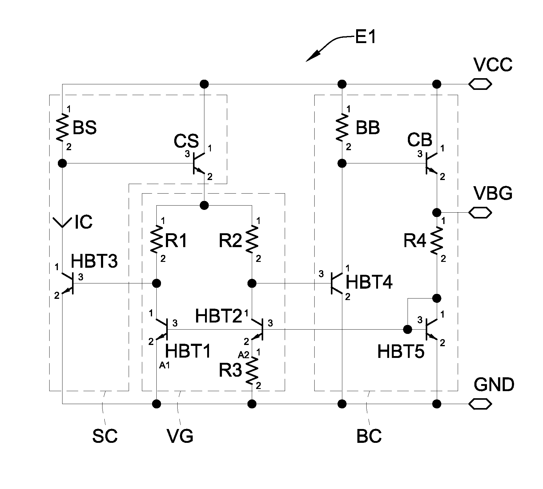
[0032]FIG. 1 shows a first embodiment E1 of a bandgap reference circuit comprising a voltage generator VG, a supply circuit SC and a bias circuit BC. The supply circuit SC and the bias circuit BC are connected to a first supply potential VCC and to a second supply potential GND. The voltage generator VG is connected to the supply circuit SC, the bias circuit BC, and the second supply potential GND. The supply voltage is the difference between the first supply potential VCC and the second supply potential GND and is equal to VCC if the second supply potential GND is chosen to be 0 V.

[0033]The voltage generator VG comprises a first, a second and a third resistor R1, R2 and R3 which each have a first connection point 1 and a second connection point 2. The first, second and third resistors R1, R2 and R3 can be thin film resistors. The first and second resistor R1 and R2 may have equal resistances. It further comprises a first and a second control element HBT1 and HBT2 which each have a ...


PUM


Abstract

Bandgap reference circuit, comprising a voltage generator (VG) designed to produce a voltage or a current proportional to absolute temperature, a supply circuit (SC), designed to produce a supply for operating the voltage generator (VG), comprising a bias element (BS) and a control element (CS), and a bias circuit (BC), designed to produce a bias for operating the voltage generator (VG), comprising a bias element (BB) and a control element (CB). At least one of the control element (CS) of the supply circuit (SC) and the control element (CB) of the bias circuit (BC) comprises a pseudomorphic high-electron-mobility transistor or a hetero-junction bipolar transistor and / or at least one of the bias element (BS) of the supply circuit (SC) and the bias element (BB) of the bias circuit (BC) comprises a long-gate pseudomorphic high-electron-mobility transistor or a resistor. Method for producing the circuit wherein the pseudomorphic high-electron-mobility transistors and the hetero-junction bipolar transistors are produced using a GaAs BiFET technology process.

Description

CROSS-REFERENCE TO RELATED APPLICATION[0001]This application is a continuation of prior International Patent Application Serial No. PCT / EP2010 / 052856, filed Mar. 5, 2010, entitled “Bandgap Reference Circuit and Method for Producing the Circuit,” which is hereby incorporated by reference herein in its entirety.COPYRIGHT[0002]A portion of the disclosure of this patent document contains material which is subject to copyright protection. The copyright owner has no objection to the facsimile reproduction by anyone of the patent disclosure, as it appears in the Patent and Trademark Office patent files or records, but otherwise reserves all copyright rights whatsoever.BACKGROUND OF THE INVENTION[0003]The invention concerns a bandgap reference circuit for providing a voltage or a current in which first order effects of temperature dependency are cancelled. Bandgap reference circuits can be used in high-frequency applications such as power amplifiers of mobile phones, which are usually manuf...

Claims


Application Information

Patent Timeline
Patent Type & Authority Patents(United States)
IPC IPC(8): G05F3/16
CPCG05F3/30
Inventor BOUWMAN, JEROENVAN DEN OEVER, LEON C. M.
Owner SNAPTRACK
Why Eureka
Try Eureka