High-brightness and anti-water-vapor-permeating printing decorative glass and production method thereof
A decorative glass and moisture-proof technology, applied in the field of decorative glass, to achieve the effect of eliminating shadows, reducing the chance of ink falling off, and improving the brightness of reflection
- Summary
- Abstract
- Description
- Claims
- Application Information
AI Technical Summary
Problems solved by technology
Method used
Image
Examples
Embodiment 1
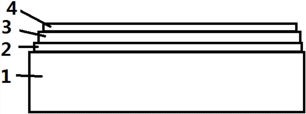
[0032] In this embodiment, the printed decorative glass includes a glass substrate and an ink pattern layer, a high-reflection film layer, and a moisture-proof protective film layer arranged on the glass substrate in sequence, wherein,
[0033] The high-reflection film layer includes an oxidized stainless steel film layer and a stainless steel film layer arranged in sequence, and the oxidized stainless steel film layer is arranged close to the ink pattern layer. At this time, the total thickness of the high reflection film layer is 32nm, that is, the total thickness of the oxide stainless steel film layer and the stainless steel film layer is 32nm.
[0034] SiO X As a protective film layer against water vapor penetration, x=1.5, and the thickness of the film layer is 25nm.
Embodiment 2
[0036] This embodiment is substantially the same as the above-mentioned Embodiment 1, the difference is that in this embodiment, the high reflection film layer includes a silicon nitride film layer, a stainless steel oxide film layer and a stainless steel film layer arranged in sequence, and the silicon nitride film layer is close to The ink pattern layer is set, wherein the total thickness of the high reflection film layer is 52nm.
[0037] SiO X As a protective film layer against water vapor penetration, x=1.65, and the thickness of the film layer is 35nm.
Embodiment 3
[0039] This embodiment is substantially the same as the above-mentioned Embodiment 1, the difference is that in this embodiment, the high reflection film layer includes a silicon oxide film layer, a stainless steel oxide film layer and a stainless steel film layer arranged in sequence, and the silicon oxide film layer is close to the ink pattern layer setting, wherein the total thickness of the high reflection film layer is 76nm.
[0040] SiO X As a protective film layer against water vapor penetration, x=1.79, and the thickness of the film layer is 45nm.
PUM
| Property | Measurement | Unit |
|---|---|---|
| thickness | aaaaa | aaaaa |
| particle diameter | aaaaa | aaaaa |
| thickness | aaaaa | aaaaa |
Abstract
Description
Claims
Application Information
 - R&D
- Intellectual Property
- Life Sciences
- Materials
- Tech Scout
- Unparalleled Data Quality
- Higher Quality Content
- 60% Fewer Hallucinations
Browse by: Latest US Patents, China's latest patents, Technical Efficacy Thesaurus, Application Domain, Technology Topic, Popular Technical Reports.
© 2025 PatSnap. All rights reserved.Legal|Privacy policy|Modern Slavery Act Transparency Statement|Sitemap|About US| Contact US: help@patsnap.com

