Semiconductor devices with reduced active region defects and unique contacting schemes

a technology of active region defects and semiconductor devices, applied in semiconductor devices, radiation controlled devices, electrical apparatus, etc., can solve the problems of low yield and high cost of v-based processing, poor absorption of si, and low cost of -based processing, so as to reduce the effect of dark curren

Inactive Publication Date: 2006-03-14
NOBLE DEVICE TECH CORP +1
View PDF13 Cites 112 Cited by
  • Summary
  • Abstract
  • Description
  • Claims
  • Application Information

AI Technical Summary

Benefits of technology

[0029]In accordance with various other embodiments of our invention, the device may be optoelectronic or electronic. In the case of optoelectronic applications, the device is a photodetector in which the first predetermined region is the active region where signal light is absorbed and a second predetermined region is a waveguide that delivers signal light to the active region. In a preferred embodiment, such a photodetector has a SiGe active region formed on a Si substrate, and as such is compatible with Si IC processing, has high speed and high QY. The photodetector may be a surface illuminated array or an edge illuminated device in which light is directed to the active region by a suitable waveguide. In electronic applications, the device is illustratively a MOSFET in which the first predetermined region includes the channel, source and drain.
[0033]In accordance with another embodiment of this aspect of our invention for use as an edge-illuminated PD, the width of the stem region (as measured transverse to the direction of light propagation) is less than half the wavelength of the signal light (as measured in the semiconductor material of the stem region), which serves to reduce penetration of the signal light therein.
[0035]In accordance with another embodiment of this aspect of our invention for use as either a surface-illuminated PD or an edge-illuminated PD, the active regions are undoped, but the stem regions are doped, thereby to reduce dark current.

Problems solved by technology

Whereas Group III–V-based processing is low yield and expensive, Si-based processing is ubiquitous and low cost.
Unfortunately Si is a poor absorber in the IR range of practical interest (e.g., 1100–1600 nm).
However, the thickness of a high quality (low defect density) single crystal Si1-xGex layer that can be grown on a single crystal Si substrate or on a Si epitaxial layer is limited by the 4% lattice constant mismatch between Si and Ge.
These defects are a source of extrinsic leakage current (dark current) that adds to the noise of the detector, thereby limiting its overall sensitivity.
As a result, near IR Si1-xGex PDs with sufficient performance cannot be made using prior art techniques to directly grow Si1-xGex on Si.
Several approaches have been proposed in the prior art in attempts to circumvent the critical layer thickness problem, but they all use complicated growth schemes.
However, the total layer structure is difficult to integrate with conventional CMOS processing because the layer stack can become quite thick and the annealing steps involved require high temperatures.
In fact, the defects exist through out the graded region.
Like the GB process, this process poses challenges to CMOS integration due to required high temperature (900 C.) anneals [See, L. Colace et al, Appl. Phys. Lett., Vol. 76, No 10, p.
However, the best material obtained by this technique still has a relatively high defect density of 2×106 cm−2.
However, prior art techniques are not capable of producing low-defect-density Ge on Si.
Otherwise, generation-recombination current results in large reverse leakage (dark) current.
It is essential that these regions be highly doped; however, it is not possible to eliminate all of the defect-induced dark current by means of high doping because some region of low-doped Ge is required to absorb the incident light signal.
These devices suffer from two important limitations: (1) process incompatibility with conventional CMOS processes, and (2) intrinsically poorer performance.
In addition, it has not previously been appreciated that these limitations are inherent in the methods of the prior art.
Because carriers are generated throughout the Ge layers, there is a distribution of transit times. Calculation of the exact frequency response is complicated, but readily done through simulation.
We have performed device simulations to assess the ideal device speed of the PIN structures discussed above and have found that the frequency response of these devices is inherently limited by transit time considerations.
It should be noted that in this structure it is not possible to reduce W indefinitely.
If this interfacial region is depleted of free carriers, prohibitively large dark currents will flow adversely impacting the noise performance.
Poor frequency response is the inherent problem in such prior art devices.
But, this design results in a frequency response limited by the diffusion time τdiff.
Consequently, in the prior art devices it is very difficult to achieve high enough f3 to satisfy the desired data rates of high-speed systems.

Method used


Image

  • Semiconductor devices with reduced active region defects and unique contacting schemes
  • Semiconductor devices with reduced active region defects and unique contacting schemes
  • Semiconductor devices with reduced active region defects and unique contacting schemes

Examples


Embodiment Construction

Fabrication Process

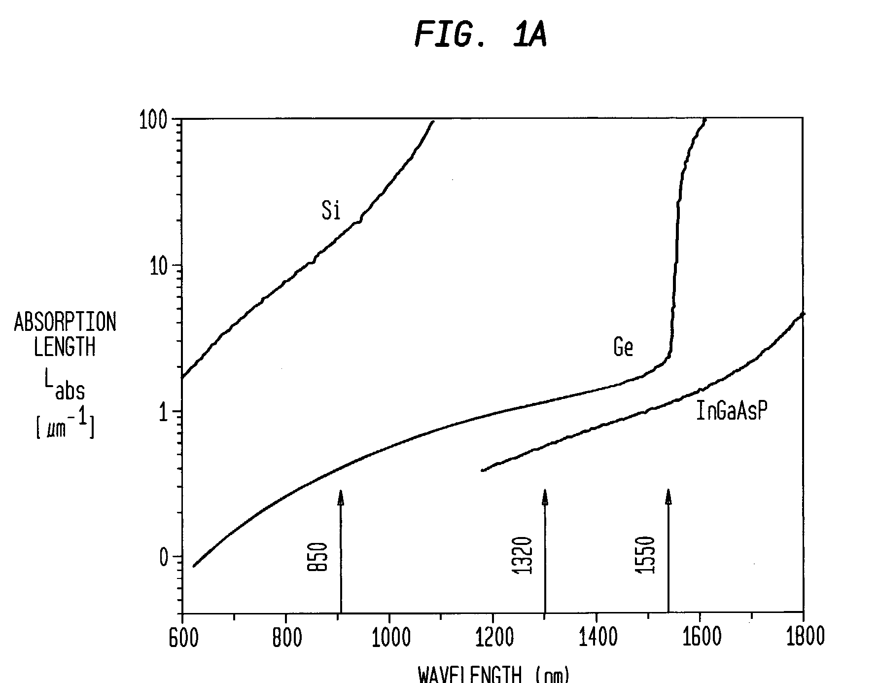
[0057]Before discussing in detail various device designs that can be realized using novel processes in accordance with one aspect of our invention, we first discuss the process as a general approach to fabricating relatively defect-free semiconductor active regions of devices such as PDs and MOSFETs. However, we concentrate in the exposition on the fabrication of low-defect-density absorption regions of SiGe PDs for operation at IR wavelengths of about 800–1600 nm for the purposes of illustration and as a reflection of one of the principal applications of our invention.

[0058]From our preceding discussion of prior art PDs, it is clear that we desire a device in which optical absorption occurs in high quality Ge, the majority of which is undoped or is depleted.

[0059]Our invention uses an epitaxial lateral overgrowth (ELO) technique to form high quality Ge embedded in an insulator structure that has been formed on top of a Si substrate. ELO has been used to monolithi...


PUM


Abstract

A method of making a semiconductor device having a predetermined epitaxial region, such as an active region, with reduced defect density includes the steps of: (a) forming a dielectric cladding region on a major surface of a single crystal body of a first material; (b) forming a first opening that extends to a first depth into the cladding region; (c) forming a smaller second opening, within the first opening, that extends to a second depth greater than the first depth and that exposes an underlying portion of the major surface of the single crystal body; (d) epitaxially growing regions of a second semiconductor material in each of the openings and on the top of the cladding region; (e) controlling the dimensions of the second opening so that defects are confined to the epitaxial regions grown within the second opening and on top of the cladding region, a first predetermined region being located within the first opening and being essentially free of defects; (D planarizing the top of the device to remove all epitaxial regions that extend above the top of the cladding layer, thereby making the top of the first predetermined region grown in the second opening essentially flush with the top of the cladding region; and (g) performing additional steps to complete the fabrication of the device. Also described are unique devices, such as photodetectors and MOSFETs, fabricated by this method, as well as unique contacting configurations that enhance their performance.

Description

CROSS-REFERENCE TO RELATED APPLICATIONS[0001]This application claims priority from provisional application Ser. No. 60 / 434,359 filed on Dec. 18, 2002.BACKGROUND OF THE INVENTION[0002]1. Field of the Invention[0003]This invention relates to semiconductor devices that have reduced active region defects and to semiconductor devices that have unique contacting schemes.[0004]2. Discussion of the Related Art[0005]Optical communication systems use near infrared (IR) radiation at wavelengths ranging from about 800 nm to 1600 nm. In particular, important communication bands are around 850 nm for short-range fiber optic communication links and around 1310 nm and 1550 nm for longer-range fiber optic communication links.[0006]Group III–V compound semiconductor photo-detectors (PDs) are currently the photodetectors of choice for optical communications receivers because GaAs-based and InP-based materials are good near IR absorbers. These detectors have absorption lengths (Labs) of about 1 μm or l...

Claims


Application Information

Patent Timeline
Patent Type & Authority Patents(United States)
IPC IPC(8): H01L27/14H01L31/00H01L31/0203H01L31/0232H01L31/117H01L21/20H01L27/146
CPCH01L27/14649H01L21/02381H01L21/02639H01L21/0262H01L21/02532H01L31/0256
Inventor BUDE, JEFFREY DEVINCARROLL, MALCOLMKING, CLIFFORD ALAN
Owner NOBLE DEVICE TECH CORP
Why Eureka
Try Eureka