FPGA debugging system and method

A debugging system and off-chip storage technology, applied in CAD circuit design, special data processing applications, instruments, etc., can solve the problems of insufficient debugging signal observation time, increase debugging signal observation time, etc., to solve the problem of inability to diagnose large time The effect of abnormal span and improving debugging efficiency

Inactive Publication Date: 2017-07-14
芯启源(南京)半导体科技有限公司
View PDF4 Cites 31 Cited by
  • Summary
  • Abstract
  • Description
  • Claims
  • Application Information

AI Technical Summary

Problems solved by technology

[0008] In view of the above-mentioned shortcoming of prior art, the object of the present invention is to provide FPGA debugging system and method, greatly increase the debugging signal observation time length, solve many problems in the prior art that cause because the debugging signal observation time length is not enough

Method used


Image

  • FPGA debugging system and method
  • FPGA debugging system and method
  • FPGA debugging system and method

Examples


specific Embodiment

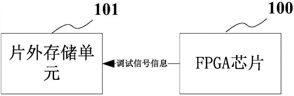
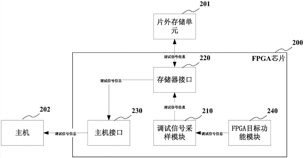
[0043] Such as figure 2 As shown, the first embodiment of the FPGA debugging system structure is shown, the off-chip memory unit 201 is connected to the FPGA chip 200 through the memory interface 220, and the memory interface 220 is connected to the debugging signal sampling module 210 in the FPGA chip 200, so The debug signal sampling module 210 is used to read the written debug signal information from the FPGA target function module 240 in the FPGA chip 200. Specifically, the FPGA target function module 240 refers to the function module that needs to be implemented originally on the FPGA , is also the debug target of the debug system, and all the debug signal information is collected from the FPGA target function module 240; the FPGA chip 200 is also connected to the host 202 through the host interface 230; wherein, the host 202 is, for example, a PC etc., the host interface 230 is, for example, any one of a PCI-E interface, a USB interface, and an Ethernet interface, and t...


PUM


Abstract

The invention provides an FPGA debugging system and method. By reading debugging signal information written by an FPGA to an off-chip storage unit with relatively large capacity and sufficient interface bandwidth for storage, the debugging signal observation time is greatly prolonged on the premise of keeping a sufficient debugging signal quantity, so that the problems of repeated selection of debugging signals and repeated try of triggering opportunities inevitable in an existing debugging mode can be avoided, the condition that a very time-consuming FPGA realization process needs to be repeatedly carried out for debugging is avoided, and the FPGA debugging efficiency is greatly improved; and the difficult problem that large-time-span exceptions cannot be diagnosed in an existing debugging technology can be solved.

Description

technical field [0001] The invention relates to the field of chip and FPGA electronic system design, in particular to an FPGA debugging system and method. Background technique [0002] Field Programmable Gate Array (FPGA) device, as a flexible and efficient programmable device, is widely used in various electronic systems and prototype verification systems for integrated circuit chip development. However, the development threshold of FPGA is relatively high, especially its debugging methods are relatively scarce. Since FPGA is running in real time and the connection channel with the host server is limited, it is impossible to use simulation verification methods to record and store the values ​​of all internal signals in real time, resulting in It is difficult to locate the cause of the abnormality after the function implemented by the FPGA design is abnormal. [0003] The main problem of the current FPGA debugging solution is that the on-chip RAM resources of the FPGA are v...

Claims


Application Information

Patent Timeline
Patent Type & Authority Applications(China)
IPC IPC(8): G06F17/50
CPCG06F30/3312G06F30/34
Inventor 袁丰磊卢笙顾沧海侯树海王俊陈安
Owner 芯启源(南京)半导体科技有限公司
Why Eureka
Try Eureka