
Evaluation apparatus and probe position inspection method

A technology for evaluation devices and probes, applied to measuring devices, parts of electrical measuring instruments, instruments, etc., can solve problems such as complex structures and non-double-sided detectors, and achieve high-precision inspection results

Active Publication Date: 2017-07-18
MITSUBISHI ELECTRIC CORP
View PDF7 Cites 5 Cited by
  • Summary
  • Abstract
  • Description
  • Claims
  • Application Information

AI Technical Summary

Problems solved by technology

The evaluation device of Patent Document 3 has a complicated structure, so it is not a structure suitable for a double-sided probe in which probes are brought into contact with both sides of a semiconductor device.

Method used


Image

  • Evaluation apparatus and probe position inspection method
  • Evaluation apparatus and probe position inspection method
  • Evaluation apparatus and probe position inspection method

Examples


Embodiment approach 1

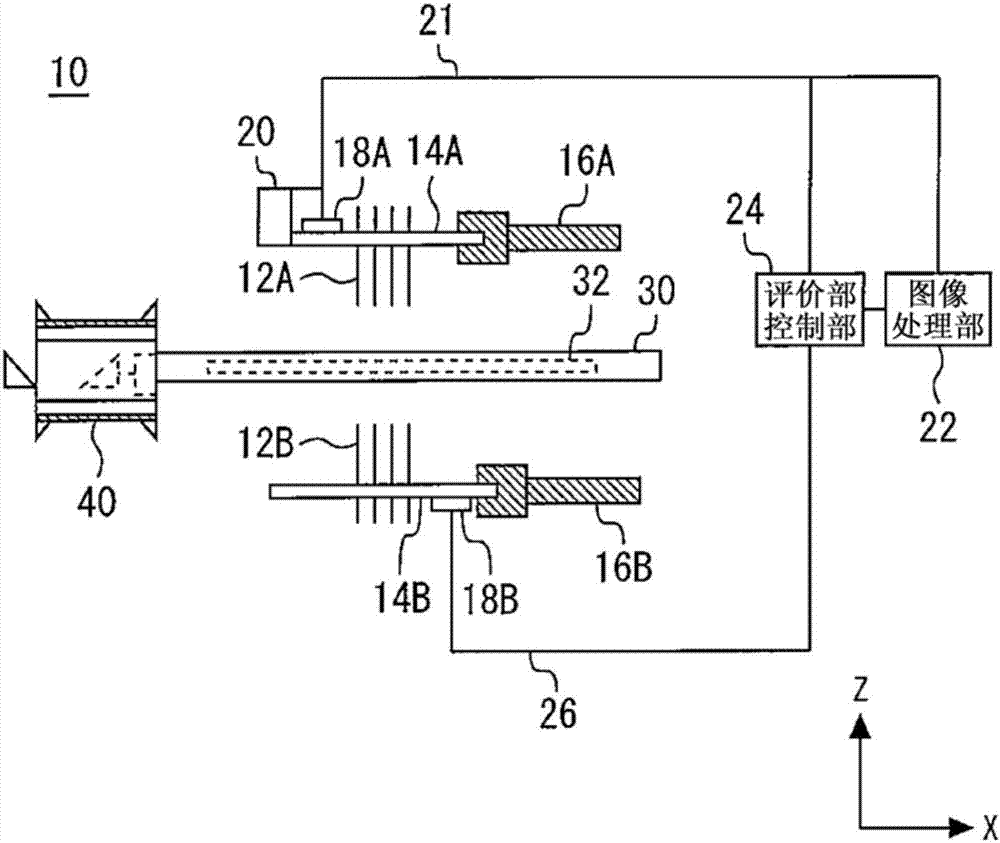
[0031] figure 1 is a front view of the evaluation device 10 . The evaluation device 10 has a first insulating plate 14A that fixes a plurality of first probes 12A, and a second insulating plate 14B that fixes a plurality of second probes 12B. 14 A of 1st insulating plates are moved in arbitrary directions by arm 16A, and 2nd insulating plate 14B is moved in an arbitrary direction by arm 16B. The first insulating plate 14A may be moved by a plurality of arms, and the second insulating plate 14B may be moved by a plurality of arms.

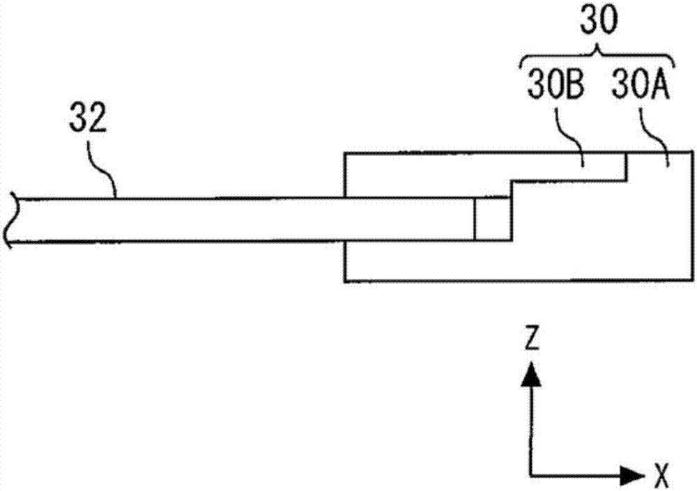
[0032] The support part 30 which fixes the semiconductor device 32 exists between the some 1st probe 12A and the some 2nd probe 12B. The support portion 30 fixes the semiconductor device 32 while exposing the upper surface and the lower surface of the semiconductor device 32 . The semiconductor device 32 is typically a semiconductor wafer on which a plurality of semiconductor chips are formed, or a semiconductor chip itself, but is not limited th...

Embodiment approach 2

[0063] Figure 9 It is a front view of the evaluation device according to Embodiment 2. The lighting 80 is attached to the 1st insulating board 14A and the 2nd insulating board 14B. The illumination 80 attached to the first insulating plate 14A irradiates in the negative z direction, and the illumination 80 attached to the second insulating plate 14B irradiates in the positive z direction. By attaching the lighting 80 to the first insulating plate 14A or the second insulating plate 14B, wiring related to the lighting can be gathered on the insulating plate.

[0064] A probe position inspection device 90 is attached to a side surface of the support portion 30 . Figure 10 It is a cross-sectional view of the probe position inspection device 90 according to the second embodiment. A reflection mirror 92 is attached to the housing 41 . The reflector 92 guides the light of the illumination 80 to the inside of the housing 41 . A transparent member 94 is provided on one surface o...


PUM


Abstract

An evaluation apparatus comprising: a supporting unit configured to fix a semiconductor device in place and cause an upper surface and a lower surface of the semiconductor device to be exposed; a first insulating plate provided above the supporting unit; a second insulating plate provided below the supporting unit; a plurality of first probes fixed to the first insulating plate; a plurality of second probes fixed to the second insulating plate; and a probe position inspection apparatus attached to the supporting unit, wherein the probe position inspection apparatus comprises: a casing including a first transparent member on a side of the first insulating plate and a second transparent member on a side of the second insulating plate; an internal prism provided in the casing; a prism rotating unit for rotating the internal prism in the casing; and an imaging unit provided outside the casing to take an image of any of the plurality of first probes contacting the first transparent member and the plurality of second probes contacting the second transparent member through the internal prism.

Description

technical field [0001] The present invention relates to an evaluation device for detecting the position of the tip of a probe and a method for checking the position of the probe. Background technique [0002] A semiconductor wafer or a chip obtained by dividing a semiconductor wafer into pieces is an object to be measured for evaluating electrical characteristics before shipment. When evaluating the electrical characteristics of the object to be measured, after the lower surface of the object to be measured is fixed on the surface of the chuck table by vacuum adsorption, etc., the probe for electrical input and output is connected to the upper surface of the object to be measured. A part of the electrode contact set. In the evaluation of a semiconductor device with a vertical structure through which a large current flows in the vertical direction, the surface of the chuck table serves as an electrode. In the evaluation of flowing a large current or applying a high voltage,...

Claims


Application Information

Patent Timeline
Patent Type & Authority Applications(China)
IPC IPC(8): H01L21/66
CPCH01L22/00H01L22/30G01R1/0408G01R1/06794G01R1/07307
Inventor 竹迫宪浩冈田章野口贵也
Owner MITSUBISHI ELECTRIC CORP
Learn More