Semiconductor device failure analysis sample and preparation method thereof, and failure analysis method

A failure analysis sample and failure analysis technology, which is applied in the field of semiconductor device failure analysis samples and their preparation, can solve the problems of uneven overall height of the surface of the sample 10, large differences in expansion coefficients, and large gradients of grinding layers, etc., to achieve improved preparation The effect of success rate, reduction of operating time, and reduction of grinding difficulty

Active Publication Date: 2017-07-21
SEMICON MFG INT TIANJIN +1
View PDF4 Cites 4 Cited by
  • Summary
  • Abstract
  • Description
  • Claims
  • Application Information

AI Technical Summary

Problems solved by technology

[0011] The inventors have found that, in addition to being time-consuming, the above-mentioned method also has the following disadvantages:
[0012] 1. Due to the soft nature of the conductive paraffin 12, the edge and surface of the sample 10 above the thick wafer 11 are easily contaminated by the conductive paraffin 12 in actual operation;
[0013] 2. Because the material of the thin sample 10 is different from that of the surrounding conductive paraffin 12, and the edge of the sample 10 has a height compared with the exposed upper surface of the thick wafer 11 (that is, the part not covered by the conductive paraffin 12 and the sample 10) Poor, this will cause the grinding speed of the edge of the sample 10 to be faster than its middle part when it is ground, which will easily cause the unevenness of the overall height of the surface of the sample 10;
[0014] 3. Due to the large difference in expansion coefficient between the conductive paraffin wax 12 and the sample 10 itself, it is easy to cause the sample 10 to bend. In the subsequent grinding process, the bending of the sample 10 will cause the gradient of the grinding level to change greatly, and the local surface of the sample 10 is very uneven. , easily broken

Method used


Image

  • Semiconductor device failure analysis sample and preparation method thereof, and failure analysis method
  • Semiconductor device failure analysis sample and preparation method thereof, and failure analysis method
  • Semiconductor device failure analysis sample and preparation method thereof, and failure analysis method

Examples


Embodiment Construction

[0062] In order to make the purpose and features of the present invention more obvious and understandable, the specific implementation of the present invention will be further described below in conjunction with the accompanying drawings. However, the present invention can be implemented in different forms and should not be limited to the described embodiments.

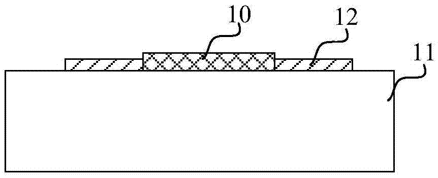
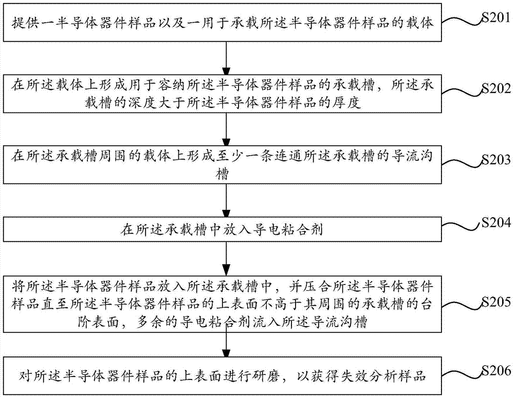
[0063] Please refer to figure 2 , this embodiment proposes a method for preparing a semiconductor device failure analysis sample, including:

[0064] S201, providing a semiconductor device sample and a carrier for carrying the semiconductor device sample;

[0065] S202, forming a bearing groove for accommodating the semiconductor device sample on the carrier, the depth of the bearing groove being greater than the thickness of the semiconductor device sample;

[0066] S203, forming at least one diversion groove communicating with the bearing groove on the carrier around the bearing groove;

[0067] S204, placing a c...


PUM


Abstract

The invention provides a semiconductor device failure analysis sample and a preparation method thereof, and a failure analysis method. A bearing groove fitting with a semiconductor device sample and at least one diversion trench communicating with the bearing groove are arranged in a carrier, a conductive adhesive is placed in the arranged bearing groove, the carrier is heated or is irradiated by ultraviolet to fuse the conductive adhesive, finally, the semiconductor device sample is placed in the bearing groove, the semiconductor device sample is lightly pressed so as to be flush with a step surface of a side wall of the bearing groove, thus pollution of the conductive adhesive to the sample surface is avoided, and more importantly, during grinding delayering, the occurrence of a phenomenon of nonuniform grinding of the sample surface is avoided.

Description

technical field [0001] The invention relates to the technical field of semiconductor device manufacturing, in particular to a semiconductor device failure analysis sample, a preparation method thereof, and a failure analysis method. Background technique [0002] Generally speaking, the failure of integrated circuits is inevitable in the process of development, production and use. With the continuous improvement of people's requirements for product quality and reliability, failure analysis is becoming more and more important. Through chip failure analysis, it can help IC designers find design defects, mismatch of process parameters, or design and operation Inappropriate and other issues. Specifically, the significance of failure analysis is mainly manifested in the following aspects: 1) failure analysis is a necessary means to determine the failure mechanism of chips; 2) failure analysis provides necessary information for effective fault diagnosis; Engineers continuously im...

Claims


Application Information

Patent Timeline
Patent Type & Authority Applications(China)
IPC IPC(8): H01L21/66
Inventor 孔云龙王潇
Owner SEMICON MFG INT TIANJIN
Why Eureka
Try Eureka