Sorting detection process and equipment used for QFN-BGA semiconductor chips

A technology of QFN-BGA and testing equipment, which is applied in semiconductor/solid-state device testing/measurement, semiconductor/solid-state device manufacturing, conveyor objects, etc. It can solve the problems of production efficiency to be improved and low degree of automation, and achieve strong functionality , high degree of automation and high sorting efficiency

Active Publication Date: 2017-07-25
TONGLING SANJIA YAMADA TECH
View PDF8 Cites 31 Cited by
  • Summary
  • Abstract
  • Description
  • Claims
  • Application Information

AI Technical Summary

Problems solved by technology

[0005] The technical problem to be solved by the present invention is that the existing sorting and testing equipment for QFN-BGA semiconductor chips is not highly auto

Method used


Image

  • Sorting detection process and equipment used for QFN-BGA semiconductor chips
  • Sorting detection process and equipment used for QFN-BGA semiconductor chips
  • Sorting detection process and equipment used for QFN-BGA semiconductor chips

Examples


Example Embodiment

[0036] The present invention will be further described below in conjunction with the drawings.

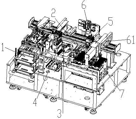
[0037] Such as figure 1 As shown, the sorting and testing equipment for QFN-BGA semiconductor chips includes a loading module 1, a workbench module 2, a thimble module 3, a suction head module 4, an array stage module 5, and a vision module 6 and receiving module 7, the material box containing the blanks is loaded on the feeding module, and the blanks are transferred between the feeding module and the workbench module through the material transfer module 61, and the ejector module The suction head module realizes the transfer, peeling and detection of the material between the workbench module and the vision module. The suction head module realizes the transfer and sorting of the chip between the vision module and the receiving module.

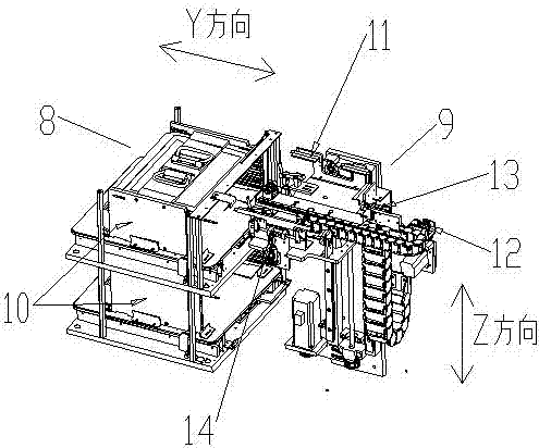
[0038] Specific, such as figure 2 As shown, the loading module may include a loading platform 8 and a material elevator 9. The loading platform include...


PUM


Abstract

The invention discloses a sorting detection process and equipment used for QFN-BGA semiconductor chips. The sorting detection equipment comprises a feeding module (1), a worktable module (2), an ejector pin module (3), a suction head module (4), an array table module (5), a visual module (6) and a material collecting module (7), wherein a material box with material sheets is loaded on the feeding module; the material sheets are conveyed between the feeding module and the worktable module through a material conveying module; conveying, stripping and detecting of the material sheets between the worktable module and the visual module can be realized through the ejector pin module and the suction head module; and conveying and sorting of the chips between the visual module and the material collecting module can be realized through the suction head module. The sorting detection process and equipment have the beneficial effects that loading of the material sheets, and stripping, detecting and sorting of the chips can be performed in an automatic manner, so that the sorting test efficiency of the QFN BGA type semiconductor chips can be realized.

Description

Technical field [0001] The invention relates to the packaging field of semiconductor chips, in particular to a sorting and testing process and equipment for QFN-BGA semiconductor chips. Background technique [0002] Semiconductor chips are widely used in computers, mobile phones, home appliances, automobiles, aerospace and other fields. They are the basic core components of electronic products. There are many types of packaging, including DIP, SOP, SOT, TSSOP, QFN, BGA, SOC, etc. According to its installation method, it is mainly divided into two types: pin and no pin. Leaded chips, such as DIP, SOP, and SOT are the early chip types and have become traditional packaging types. Their separation processing is to use a cutting rib forming equipment to peel the products one by one from the lead frame, and Bend the pins into corresponding pin shapes. This kind of molding equipment has been widely used in semiconductor packaging and testing manufacturers. In recent years, as the volu...

Claims


Application Information

Patent Timeline
IPC IPC(8): H01L21/66H01L21/67H01L21/677H01L21/683
CPCH01L21/67271H01L21/67781H01L21/6835H01L21/6838H01L22/12H01L22/20
Inventor 张青松陈迎志丁宁
Owner TONGLING SANJIA YAMADA TECH
Why Eureka
Try Eureka