
Field effect transistor

A field-effect transistor, nitride semiconductor technology, applied in transistors, semiconductor devices, electric solid-state devices, etc., can solve the problems of unstable operation and long distance.

Inactive Publication Date: 2017-08-01
SHARP KK
View PDF7 Cites 1 Cited by
  • Summary
  • Abstract
  • Description
  • Claims
  • Application Information

AI Technical Summary

Problems solved by technology

Therefore, in the case of this structure, there is a problem that the distance between the gate and the source is extremely long especially at the end, and stable operation cannot be performed due to the influence of parasitic resistance and noise.

Method used


Image

  • Field effect transistor
  • Field effect transistor
  • Field effect transistor

Examples


no. 1 approach

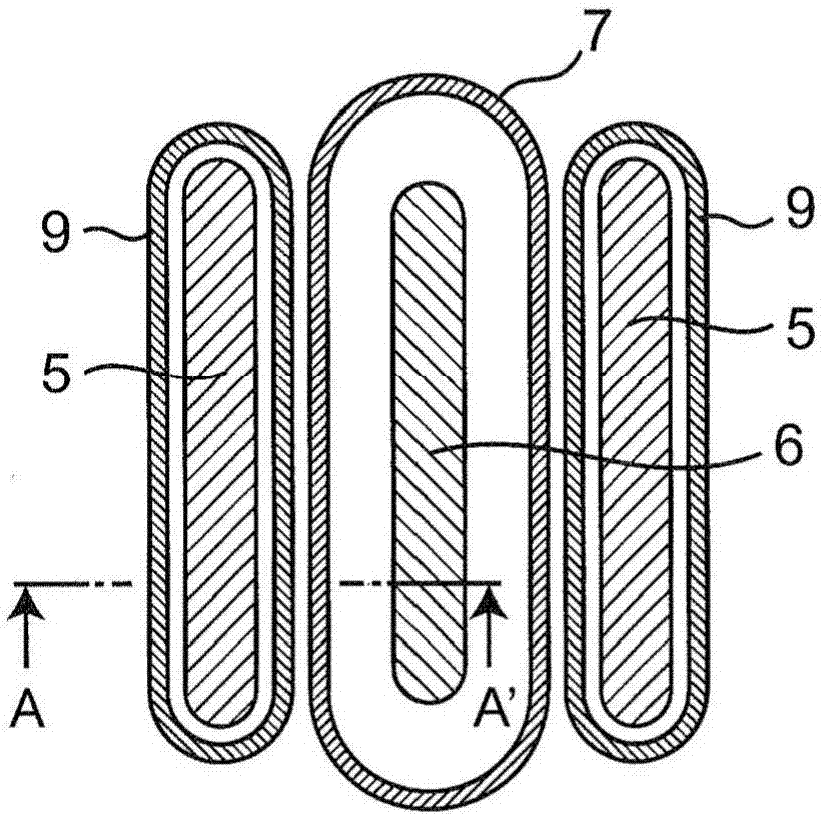
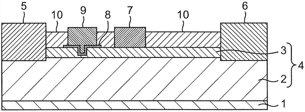
[0043] figure 1 is a plan view of a nitride semiconductor HFET as a field effect transistor of the first embodiment, figure 2 for figure 1 The cross-sectional view of the A-A' arrow.

[0044] The nitride semiconductor HFET as figure 2 As shown, on a substrate 1 made of Si, a channel layer 2 made of GaN and a channel layer made of Al are sequentially formed. x Ga 1-x A barrier layer 3 composed of N (0x Ga 1-x The Al mixed crystal ratio x of N is set to x=0.17 as an example. Then, 2DEG (two dimensional electrons: two-dimensional electron gas) is generated at the interface between the channel layer 2 and the barrier layer 3 . In the present embodiment, the nitride semiconductor 4 is constituted by the channel layer 2 and the barrier layer 3 . In addition, in this embodiment, as an example, the thickness of the barrier layer 3 is set to 30 nm.

[0045] On the barrier layer 3 , a source electrode 5 and a drain electrode 6 are formed with a preset interval. In the present...

no. 2 approach

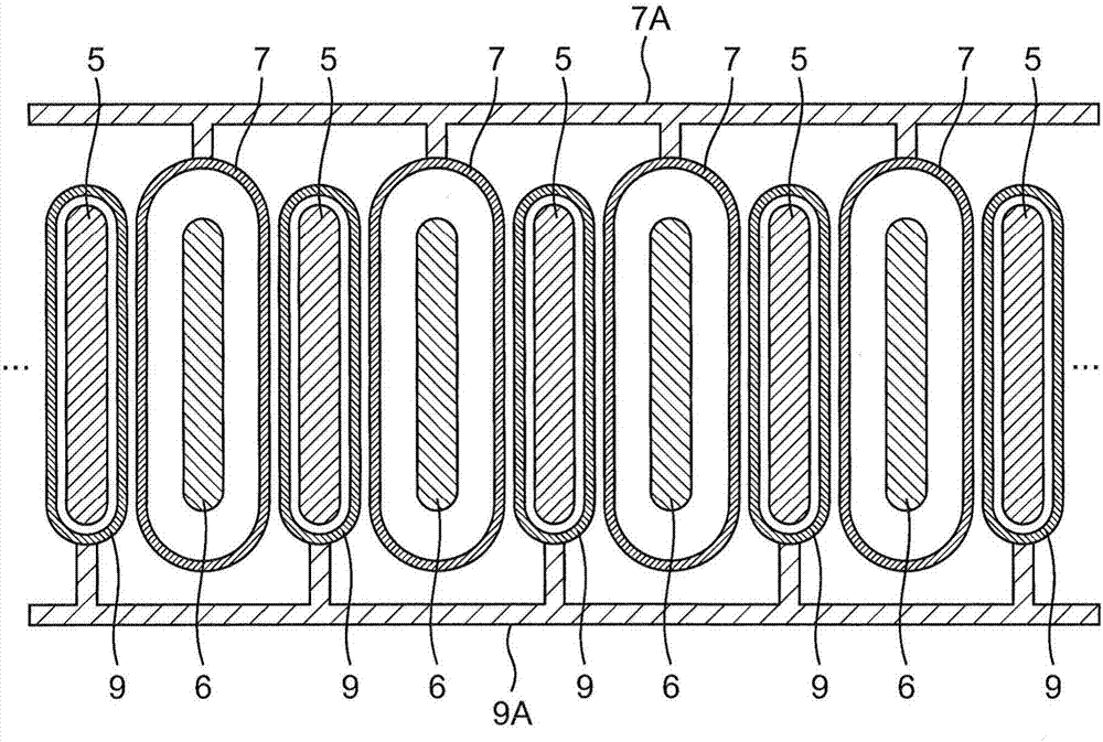
[0064] image 3 It is a plan view of a nitride semiconductor HFET as a field effect transistor of the second embodiment.

[0065] The nitride semiconductor HFET, towards the image 3 The cross section in the direction perpendicular to the extending direction of the drain electrode 6 has the same figure 2Exactly the same structure. Here, the same reference numerals are assigned to the same components as in the first embodiment, and detailed description thereof will be omitted. Hereinafter, points different from the case of the first embodiment will be described.

[0066] In this embodiment, if image 3 As shown, in plan view, in the direction perpendicular to the extending direction of the drain electrode 6, a plurality of figure 1 The structure of the nitride semiconductor HFET of the first embodiment is shown. Then, at one of the two ends of the first gate electrode 7 of each nitride semiconductor HFET, a first gate electrode wiring 7A commonly connected to each first ...

no. 3 approach

[0070] Figure 4 It is a plan view of a nitride semiconductor HFET as a field effect transistor of the third embodiment.

[0071] The nitride semiconductor HFET, towards the Figure 4 The cross-section in the direction perpendicular to the extending direction of the drain electrode 6 has the same figure 2 Exactly the same structure. Here, the same reference numerals are assigned to the same components as in the first embodiment, and detailed description thereof will be omitted. Hereinafter, points different from those of the first and second embodiments will be described.

[0072] In this embodiment, if Figure 4 As shown, when viewed from above, the distance L1 between the first gate electrode 7 and the drain electrode 6 in normal conduction operation at the end is set to be the same as the distance L2 to the straight line portion or to be larger than the distance L2 at the straight line. The distance to L2 is longer.

[0073] Also in the said end part, the electric fi...


PUM


Abstract

This field effect transistor is provided with: a nitride semiconductor layer that includes a heterojunction; a source electrode (5) and drain electrode (6) that are disposed, with a space therebetween, on the nitride semiconductor layer; a first gate electrode (7) that is positioned between the source electrode (5) and the drain electrode (6) and operates in a normally on state; and a second gate electrode (9) that is positioned between the first gate electrode (7) and the source electrode (5) and operates in a normally off state. The first gate electrode (7) is disposed so as to surround the drain electrode (6) when seen in plan view, and the second gate electrode (9) is disposed so as to surround the source electrode (5) when seen in plan view.

Description

technical field [0001] The present invention relates to a field-effect transistor having a nitride semiconductor HFET (heterostructure field-effect transistor: heterojunction field-effect transistor) structure. Background technique [0002] In the above-mentioned nitride semiconductor device having the HFET structure, normally-on (conducting state at a gate voltage of 0 volts) operation is generally performed at a practical level. However, in order to operate safely without current flowing even when the control of the gate voltage is abnormal, normally-off (normally-off) operation is strongly desired. [0003] However, even if the normally-off operation can be realized, the gate withstand voltage is as low as several tens of volts. In the field of power supply devices, it is very difficult to realize a gate withstand voltage of several hundreds of volts or more, but it is very difficult to achieve a sufficient gate withstand voltage. [0004] Here, a method is proposed in ...

Claims


Application Information

Patent Timeline
Patent Type & Authority Applications(China)
IPC IPC(8): H01L21/338H01L21/336H01L21/337H01L27/095H01L29/06H01L29/417H01L29/778H01L29/78H01L29/808H01L29/812
CPCH01L29/41725H01L29/4236H01L29/4238H01L29/7786H01L29/0619H01L21/8252H01L27/085H01L27/0605H01L29/2003H01L29/1066H01L29/402H01L29/42316H01L29/7787
Inventor 永久哲三福见公孝吐田真一
Owner SHARP KK
Learn More