A Wiring Method of Adder Supporting Pin Swapping

A wiring method and adder technology, applied in the direction of logic circuits using specific components, can solve the problems of reducing the success rate of wiring and increasing the complexity of wiring, so as to improve the bypassability, improve chip utilization, and save logic resources. Effect

Active Publication Date: 2020-08-14
CAPITAL MICROELECTRONICS
View PDF6 Cites 0 Cited by
  • Summary
  • Abstract
  • Description
  • Claims
  • Application Information

AI Technical Summary

Problems solved by technology

[0004] In the FPGA chip, due to the limitations of the FPGA chip and the hardware architecture of the full adder, usually only a relatively small number of winding paths can be connected from the XBAR, which limits the number of input signals and increases the complexity of wiring. degree, reducing the success rate of wiring

Method used


Image

  • A Wiring Method of Adder Supporting Pin Swapping
  • A Wiring Method of Adder Supporting Pin Swapping
  • A Wiring Method of Adder Supporting Pin Swapping

Examples


Embodiment Construction

[0022] The technical solutions of the present invention will be described in further detail below with reference to the accompanying drawings and embodiments.

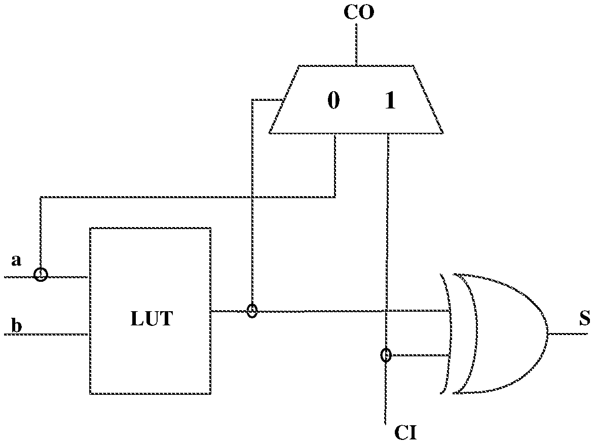
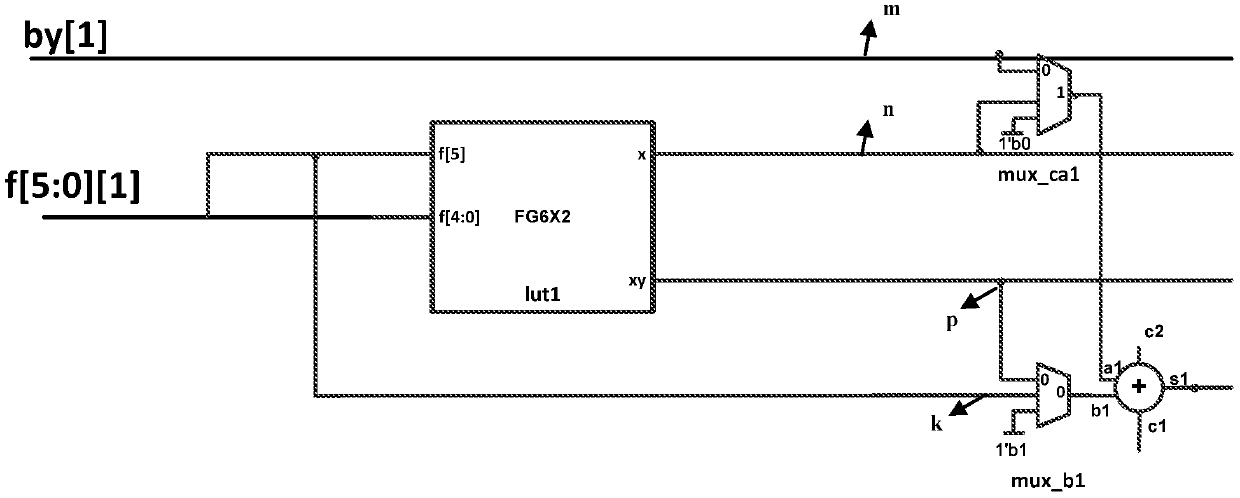
[0023] The methods in the following embodiments of the present invention are implemented based on the first chip C1 of the cloud series in the FPGA chip. figure 2 A schematic structural diagram of a programmable logic module in a C1 architecture provided by an embodiment of the present invention. C1 is the first chip of the cloud series in the FPGA chip, mainly used in the field of high-speed communication. Such as figure 2 As shown, in the structure of PLB (Programmable Logic Block, programmable logic module), the a1 terminal of the full adder ADD1 can input the signal m connected from the outside of the PLB, the signal n output from the front LUTx, or the constant connected 0 / 1; its b1 input terminal can input the signal k of f5 from the outside of the PLB, the signal p of the xy output of the front LUT, or acces...


PUM


Abstract

An adder wiring method supporting pin swapping. The method comprises: locking a full adder, and determining that at least one input end in the full adder needs to receive an input signal (m) from the outside of a PLB; determining whether a first look-up table (LUT1) has an unused input end (F4); where the unused input end exists, switching the input signal (m) from the outside of the PLB to the unused input end (F4) of the first look-up table (LUT1); and connecting an output end (x) of the look-up table to at least one input end (a) of the full adder. According to the wiring method, a pin swapping technique is extended to a full adder based on a chip architecture of C1. By using the full adder, logical resources are saved, and the utilization rate of a chip is effectively improved. At the same time, with the aid of interchangeability of two input port pins of the full adder and unused input and output ports of a front end LUT, connectivity and fmax of the full adder are improved by means of the pin swapping technique, and the full adder can select a pathway for wiring, thereby expanding a solution space for wiring, and reducing the overall power consumption of the chip.

Description

technical field [0001] The invention relates to the technical field of integrated circuits, in particular to an adder wiring method supporting pin exchange. Background technique [0002] Field-Programmable Gate Array (Field-Programmable Gate Array, FPGA) is a logic device with abundant hardware resources, powerful parallel processing capability and flexible reconfigurable capability. These features make FPGA more and more widely used in data processing, communication, network and many other fields. [0003] As a basic operation, addition is widely used in various algorithms of digital signal processing and digital communication. Because the adder is used frequently, its speed often affects the operating rate of the entire system. Inside an FPGA, an adder is usually implemented by a carry chain. figure 1 It is a schematic diagram of the logical structure of the full adder in the prior art, such as figure 1 As shown, the full adder includes a look-up table LUT (Look-Up Tab...

Claims


Application Information

Patent Timeline
Patent Type & Authority Patents(China)
IPC IPC(8): H03K19/02
CPCH03K19/02
Inventor 耿嘉
Owner CAPITAL MICROELECTRONICS
Why Eureka
Try Eureka