Method for checking consistency of schematic diagram and PCB production data

A technology of production data and schematic diagrams, applied in the field of electronic information, can solve problems such as production scrap, functional failure, project delay, etc., to achieve the effect of saving time, cost and simple operation

Active Publication Date: 2017-08-08
P C B A ELECTRONICS WUXI
View PDF4 Cites 33 Cited by
  • Summary
  • Abstract
  • Description
  • Claims
  • Application Information

AI Technical Summary

Problems solved by technology

The schematic diagram is a file output by the user, which includes hardware function description, device BOM (bill of materials), and is converted into electronic PCB design data through the network. After completing the PCB design data and inspection, data processing before processing is required. However, in the electronic version In the two processes of PCB data design and pre-process data processing, the hardware connection relationship may cause hardware connection errors due to the professional level of the designer, operational errors, software bugs, etc.
Usually these two processes are difficult to control, and the schematic diagram cannot be traced to the PCB process process, which may lead to omissions in the intermediate process, resulting in production scrap
In the industry, similar quality accidents occur frequently, leading to serious accidents such as project delays and functional failures
The current commonly used method is IPC network comparison, but the limitation is that the content of IPC comparison is the PCB design data network and PCB production data network, which cannot cover the schematic diagram link

Method used


Image

  • Method for checking consistency of schematic diagram and PCB production data

Examples


Embodiment Construction

[0017] The present invention will be further described below in conjunction with drawings and embodiments. It should be understood that the specific embodiments described here are only used to explain the present invention, but not to limit the present invention. In addition, it should be noted that, for the convenience of description, only some parts related to the present invention are shown in the accompanying drawings but not the whole content. Unless otherwise defined, all technical and scientific terms used herein are related to the technical field of the present invention. The skilled person generally understands the same meaning. The terms used herein are for describing specific embodiments only, and are not intended to limit the present invention.

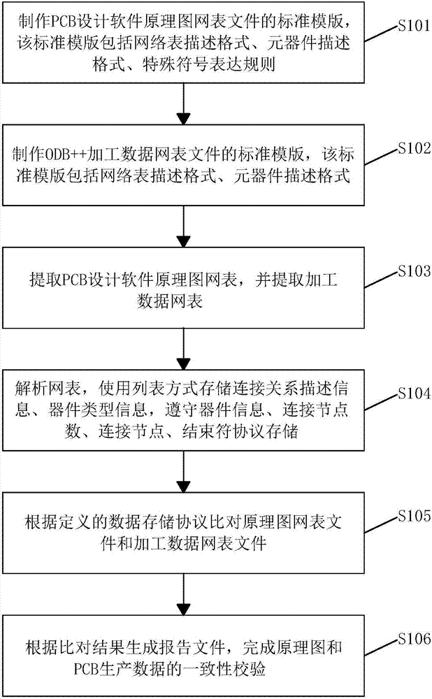
[0018] Please refer to figure 1 as shown, figure 1 The flow chart of the method for verifying the consistency of the schematic diagram and PCB production data provided by the present invention.

[0019] In this embodim...


PUM


Abstract

The invention discloses a method for checking consistency of a schematic diagram and PCB production data. The method comprises steps as follows: making a standard template of a PCB design software schematic diagram netlist file; making a standard template of an ODB++processing data netlist file; extracting a PCB design software schematic diagram netlist, and extracting a processing data netlist; analyzing the netlists, and storing connecting relation description information, device type information, abidance device information, connection node number, connection nodes and a terminator protocol in a list manner; comparing theschematic diagram netlist file with the processing data netlist file according to a defined data storage protocol; generating a report file according to a comparison result. According to the method, the problems of network loss, short circuit and the like caused by negligence, software bug and the like in a PCB design process are solved, time cost consumed by a designer for connecting relation correction is saved, and the method is better than a currently utilized IPC (inter-process communication) netlist comparison method in the aspects of accuracy and efficiency.

Description

technical field [0001] The invention relates to the technical field of electronic information, in particular to a method for verifying the consistency of schematic diagrams and PCB production data. Background technique [0002] The process of conventional PCB printed board design and processing is the process from schematic diagram input to printed board output, from logical description to physical realization. The schematic diagram is a file output by the user, which includes hardware function description, device BOM (bill of materials), and is converted into electronic PCB design data through the network. After completing the PCB design data and inspection, data processing before processing is required. However, in the electronic version In the two processes of PCB data design and pre-process data processing, the hardware connection relationship may cause hardware connection errors due to the designer's professional level, operational errors, and software bugs. Usually, t...

Claims


Application Information

Patent Timeline
Patent Type & Authority Applications(China)
IPC IPC(8): G06F17/50
CPCG06F30/398
Inventor 应朝晖陈懿陈传开陈锡波姚景升靳浪平
Owner P C B A ELECTRONICS WUXI
Why Eureka
Try Eureka