Eureka AIR delivers breakthrough ideas for toughest innovation challenges, trusted by R&D personnel around the world.

Electronic package

An electronic package and electronic component technology, which is applied in the directions of electrical components, electrical solid devices, and printed electrical components, etc., can solve the problem of difficult integrated production, the inability to miniaturize the wireless communication module 1, and the difficulty in reducing the width of the wireless communication module 1. And other issues

Inactive Publication Date: 2017-08-11
SILICONWARE PRECISION IND CO LTD
View PDF6 Cites 10 Cited by
  • Summary
  • Abstract
  • Description
  • Claims
  • Application Information

AI Technical Summary

Problems solved by technology

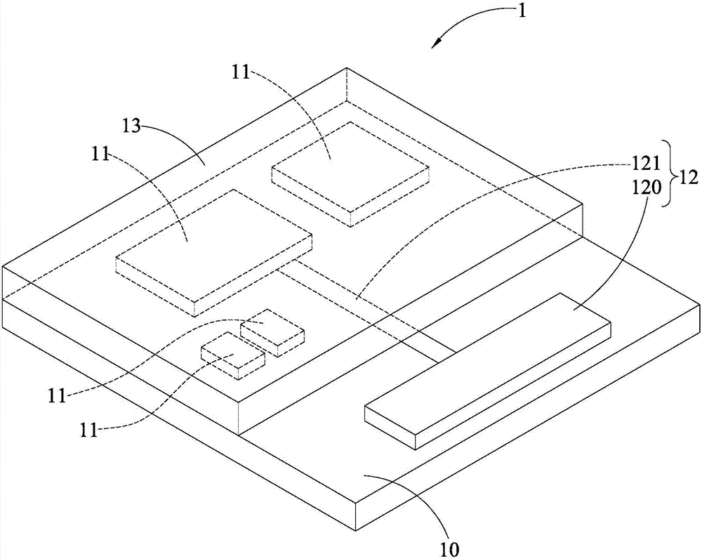
[0004] In the aforementioned known wireless communication module 1, since the antenna structure 12 is planar, based on the electromagnetic radiation characteristics between the antenna structure 12 and the electronic component 11 and the volume limitation of the antenna structure 12, during the manufacturing process, The antenna body 120 is difficult to integrate with the electronic component 11, that is, the encapsulant 13 only covers the electronic component 11, but does not cover the antenna body 120, so that the mold for the packaging process needs to correspond to the layout area of ​​the plurality of electronic components 11 , rather than corresponding to the size of the packaging substrate 10, which is not conducive to the packaging process
[0005] In addition, because the antenna structure 12 is planar, it is necessary to increase the layout area (the area where the encapsulant 13 is not formed) on the surface of the package substrate 10 to form the antenna body 120, making it difficult to reduce the width of the package substrate 10. Therefore, it is difficult to reduce the width of the wireless communication module 1, so that the wireless communication module 1 cannot meet the requirement of miniaturization

Method used


Image

  • Electronic package
  • Electronic package
  • Electronic package

Examples


Embodiment Construction

[0045] The implementation of the present invention is described below through specific specific examples, and those skilled in the art can easily understand other advantages and effects of the present invention from the content disclosed in this specification.

[0046] It should be noted that the structures, proportions, sizes, etc. shown in the drawings attached to this specification are only used to match the content disclosed in the specification, for the understanding and reading of those familiar with this technology, and are not used to limit the implementation of the present invention Therefore, it has no technical substantive meaning. Any modification of structure, change of proportional relationship or adjustment of size shall still fall within the scope of this invention without affecting the effect and purpose of the present invention. The technical content disclosed by the invention must be within the scope covered. At the same time, terms such as "above", "first",...


PUM


Abstract

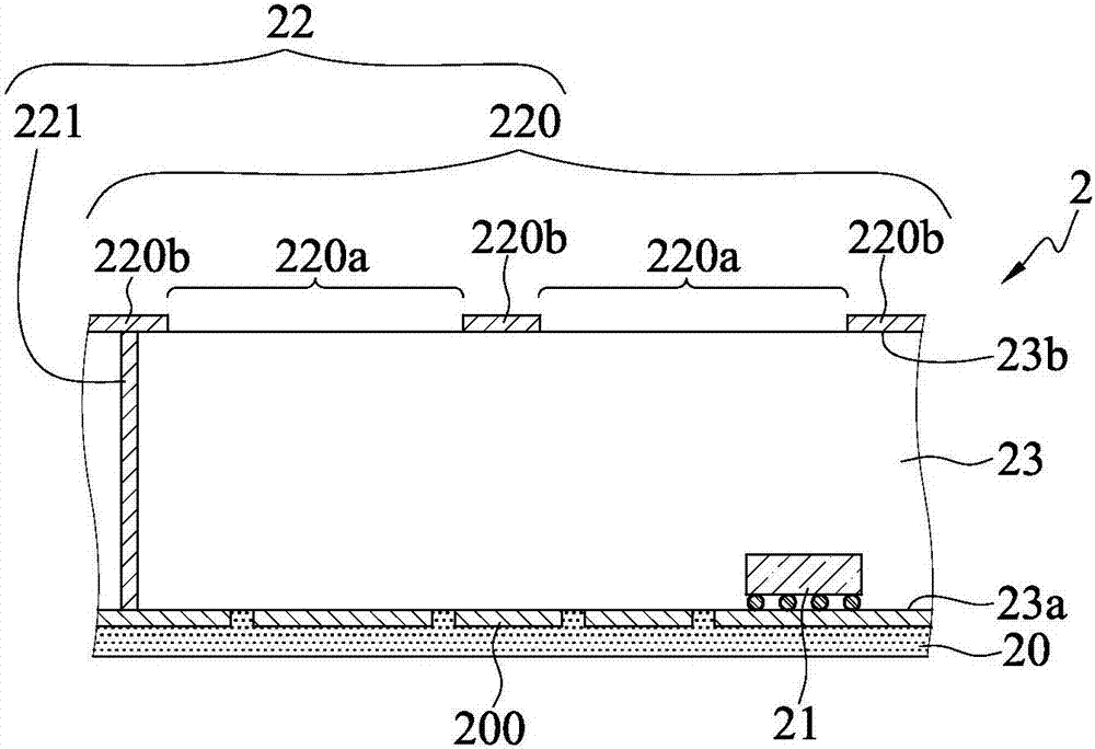
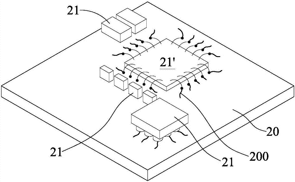
An electronic package is provided, which includes: a substrate, an electronic element disposed on the substrate, and an antenna structure disposed on the substrate. The antenna structure has a base portion and at least a support portion, the base portion including a plurality of openings and a frame separating the openings from one another, and the support portion supporting the base portion over the substrate. Therefore, no additional area is required to be defined on a surface of the substrate, and the miniaturization requirement of the electronic package is thus met.

Description

technical field [0001] The invention relates to an electronic package, especially an electronic package with an antenna structure. Background technique [0002] With the vigorous development of the electronic industry, wireless communication technology has been widely used in various consumer electronic products to facilitate receiving or sending various wireless signals. In order to meet the appearance design requirements of consumer electronics products, the manufacture and design of wireless communication modules are developed towards light, thin, short and small requirements. Among them, the planar antenna (Patch Antenna) is small in size, light in weight and easy to manufacture. and other characteristics and are widely used in wireless communication modules of electronic products such as cell phones and personal digital assistants (PDA). [0003] figure 1 It is a three-dimensional schematic diagram of the wireless communication module. Such as figure 1 As shown, the...

Claims


Application Information

Patent Timeline
Patent Type & Authority Applications(China)
IPC IPC(8): H01L23/66H01Q1/22
CPCH01L23/66H01Q1/2283H01L2223/6677G06K19/07777H05K1/165H05K1/186H05K3/0014H05K3/107H05K3/207H05K3/4602H05K3/465H01L2224/16225H01L2224/48091H01L2924/1815H05K2201/09118H05K2203/1327H01L25/16H01Q1/38H05K2201/10098H01L2924/00014H05K1/185H01L25/00
Inventor 邱志贤陈嘉扬卢盈维张峻源蔡明汎
Owner SILICONWARE PRECISION IND CO LTD
Why Eureka
Eureka Blog
Learn More