High voltage metal oxide semiconductor transistor and fabricating method thereof

a metal oxide semiconductor and high-voltage technology, applied in the direction of transistors, semiconductor devices, electrical appliances, etc., can solve the problems of unnecessary current leakage and increase of sub-threshold current, and achieve the effect of avoiding leakage current and lowering the sub-threshold current of the mos devi

Active Publication Date: 2009-02-03
UNITED MICROELECTRONICS CORP
View PDF3 Cites 7 Cited by
  • Summary
  • Abstract
  • Description
  • Claims
  • Application Information

AI Technical Summary

Benefits of technology

[0007]Accordingly, one objective of the present invention is to provide a high voltage metal-oxide-semiconductor (MOS) transistor and fabricating method thereof capable of avoiding the leakage current and lowering the sub-threshold current of the MOS device.
[0023]In the present invention, the width of the gate of the high voltage MOS transistor is smaller than or at most equal to that of the drift regions and the width of the channel region is greater than that the drift regions. Hence, the leakage current flowing from the edge of the gate can be reduced and the sub-threshold voltage resulted from a short channel width can be avoided.

Problems solved by technology

One major disadvantage for this layout is that when the width of the device is smaller, charges in the source region 140a can easily flow from the drift region 120a along the edge of the gate 150 into the drift region 120b, leading to unnecessary current leakage.
However, one major problem for this layout is that the sub-threshold current will increase following a reduced dimension of the device.

Method used


Image

  • High voltage metal oxide semiconductor transistor and fabricating method thereof
  • High voltage metal oxide semiconductor transistor and fabricating method thereof
  • High voltage metal oxide semiconductor transistor and fabricating method thereof

Examples


Embodiment Construction

[0030]Reference will now be made in detail to the present embodiments of the invention, examples of which are illustrated in the accompanying drawings. Wherever possible, the same reference numbers are used in the drawings and the description to refer to the same or like parts.

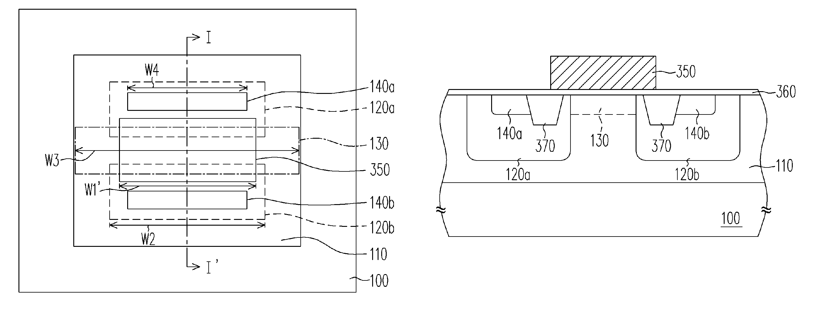
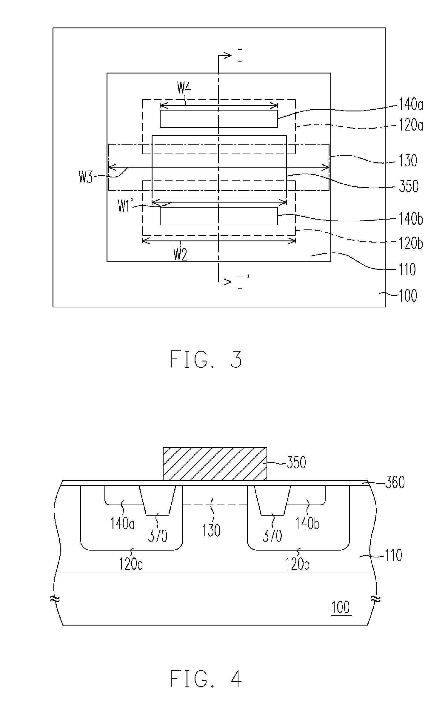
[0031]FIG. 3 is a top view of a high voltage metal-oxide-semiconductor (MOS transistor according to one embodiment of the present invention. FIG. 4 is a schematic cross-sectional view along line I-I′ of the high voltage MOS transistor in FIG. 3. As shown in FIGS. 3 and 4, the high voltage MOS transistor of the present invention comprises a substrate 100, a well 110, two drift regions 120a / 120b, a channel region 130, a source / drain region 140a / 140b, an isolation structure 370, a gate insulation layer 360 and a gate 350. The well 110 is disposed in the substrate 100. The gate insulation layer 360, made of silicon oxide, for example, is disposed over the substrate 100. The gate 350, made of doped polysilicon, for...


PUM


Abstract

A high voltage MOS transistor including a substrate, a well, a gate insulation layer, a gate, two drift regions, a channel region, a source / drain region and an isolation structure is provided. The well is disposed in the substrate and the gate insulation layer is disposed over the substrate. The gate is disposed over the gate insulation layer. The two drift regions are in the well at two sides of the gate and the width of the gate is smaller than or equal to that of the drift regions. The channel region is disposed between the drift regions and the width of the channel region is greater than that of the drift regions. The source / drain regions are formed within the drift regions. The isolation structure is disposed inside the drift regions between the source / drain region and the channel region. The drift regions enclose the source / drain regions and the isolation structure.

Description

BACKGROUND OF THE INVENTION[0001]1. Field of the Invention[0002]The present invention relates to a metal-oxide-semiconductor (MOS) transistor and fabricating method thereof. More particularly, the present invention relates to a high voltage MOS transistor and fabricating method thereof.[0003]2. Description of the Related Art[0004]High voltage metal-oxide-semiconductor (MOS) transistors are widely used in electronic products that require high voltage, such as flash memory or the control circuit of a flat panel display. Since the high voltage MOS transistor must operate at a high voltage without any signs of electrical breakdown, the breakdown voltage of a high voltage MOS transistor is higher than most conventional devices.[0005]FIG. 1 is a top view of a conventional high voltage metal-oxide-semiconductor (MOS) transistor. As shown in FIG. 1, the high voltage MOS transistor 100 mainly comprises a substrate 100, a well 110, two drift regions 120a / 120b, two source / drain regions 140a / 14...

Claims


Application Information

Patent Timeline
Patent Type & Authority Patents(United States)
IPC IPC(8): H01L29/76
CPCH01L29/0653H01L29/0692H01L29/1033H01L29/42372H01L29/66568H01L29/7833
Inventor CHEN, HWI-HUANG
Owner UNITED MICROELECTRONICS CORP
Why Eureka
Try Eureka