Crystalline film, device, and manufacturing methods for crystalline film and device

Inactive Publication Date: 2013-03-14
NAMIKI SEIMITSU HOSEKI KK +1
View PDF9 Cites 7 Cited by
  • Summary
  • Abstract
  • Description
  • Claims
  • Application Information

AI Technical Summary

Benefits of technology

[0037]According to the present invention described above, it becomes possible to control the warpage shape of the crystalline film subjected to double-sided polishing, which has such a thickness that the crystalline film is capable of free-standing, and to obtain the crystalline film in which the warpage amount is reduced or eliminated with high precision. Consequently, through flattening of the crystalline film, it becomes possible to facilitate a subsequent step, and reduce or eliminate variations in crystal axis angle inside the crystalline film.
[0038]In addition, through the use of the pulsed laser, it is possible to concentrate energy in a short time width to obtain a high peak output, and hence the use of the pulsed laser is preferable for the formation of the reformed region pattern and, by the irradiation condition and irradiation position of the pulsed laser, it is possible to uniquely control the warpage amount, and hence it becomes possible to shorten the step of reducing or eliminating the warpage amount as compared with a conventional step.
[0039]Further, when the relative position of the reformed region pattern in the thickness direction of the crystalline film is assumed to be 0% at one surface of the crystalline film as a reference value and 100% at the other surface thereof, the reformed region pattern is formed in the range of 3% or more and 95% or less, and further in the range of 3% or more and less than 50% in the thickness direction of the crystalline film. In this manner, it is possible to form the reformed region pattern without affecting the surface of the crystalline film, and also reduce or eliminate the warpage amount occurring in the crystalline film subjected to double-sided po

Problems solved by technology

However, the substrate for growth and the crystalline film have different lattice constants and different thermal expansion coefficients, and hence it has been extremely difficult to grow the crystalline film to such a thickness that the crystalline film is capable of free-standing (for example, 300 μm or more).
However, even when the crystalline film could be grown to such a thickness that the crystalline film is capable of free-standing, there has been a problem in that, in the process of separating the substrate for growth from the crystalline film, an internal strain resulting from differences in thermal expansion coefficient and lattice constant between the substrate

Method used


Image

  • Crystalline film, device, and manufacturing methods for crystalline film and device
  • Crystalline film, device, and manufacturing methods for crystalline film and device
  • Crystalline film, device, and manufacturing methods for crystalline film and device

Examples


Embodiment Construction

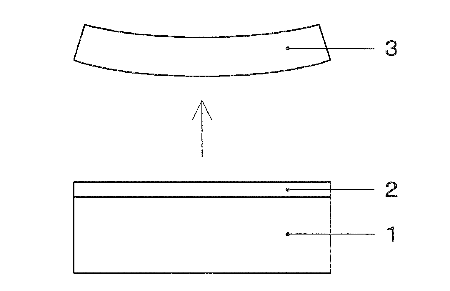
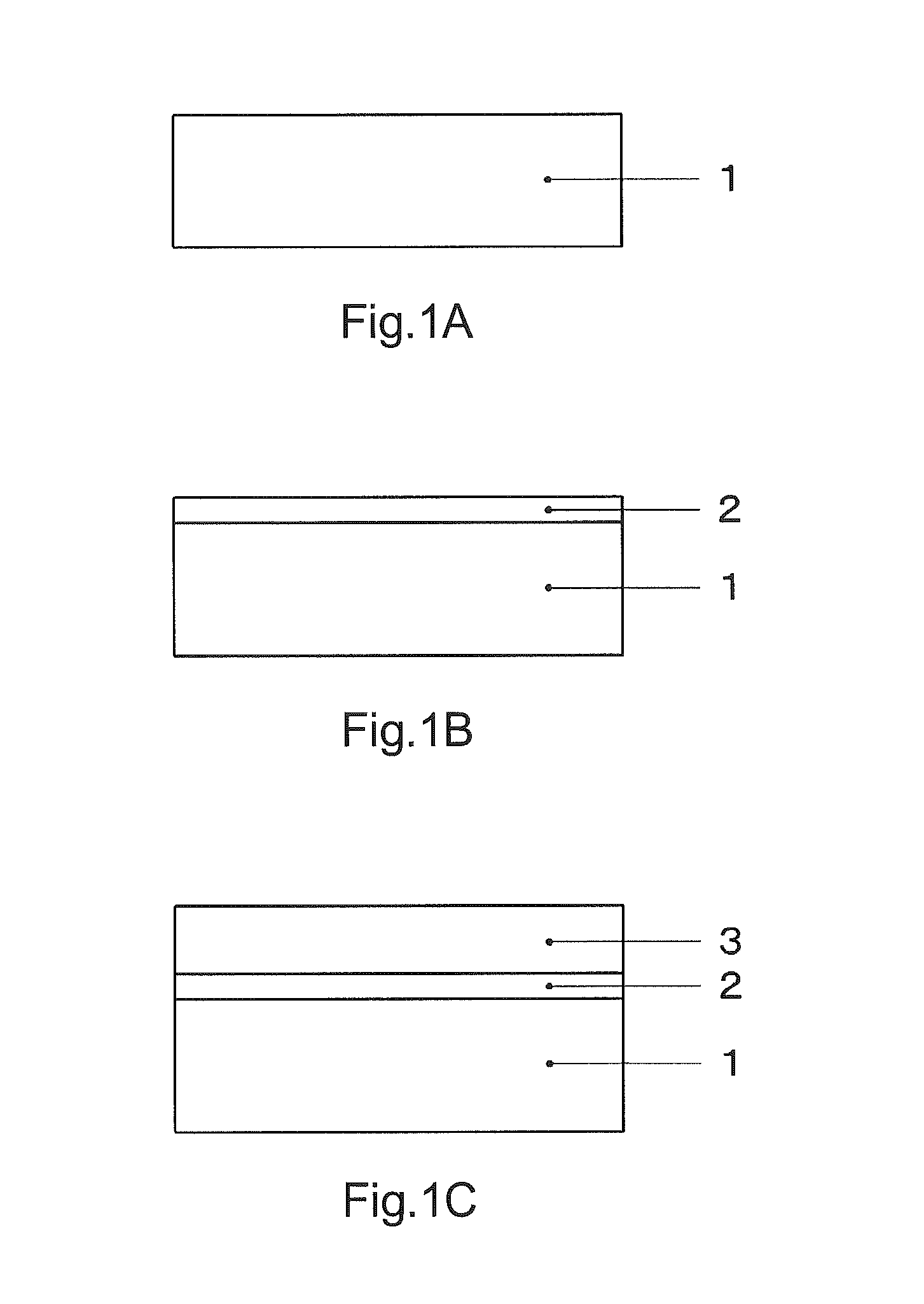
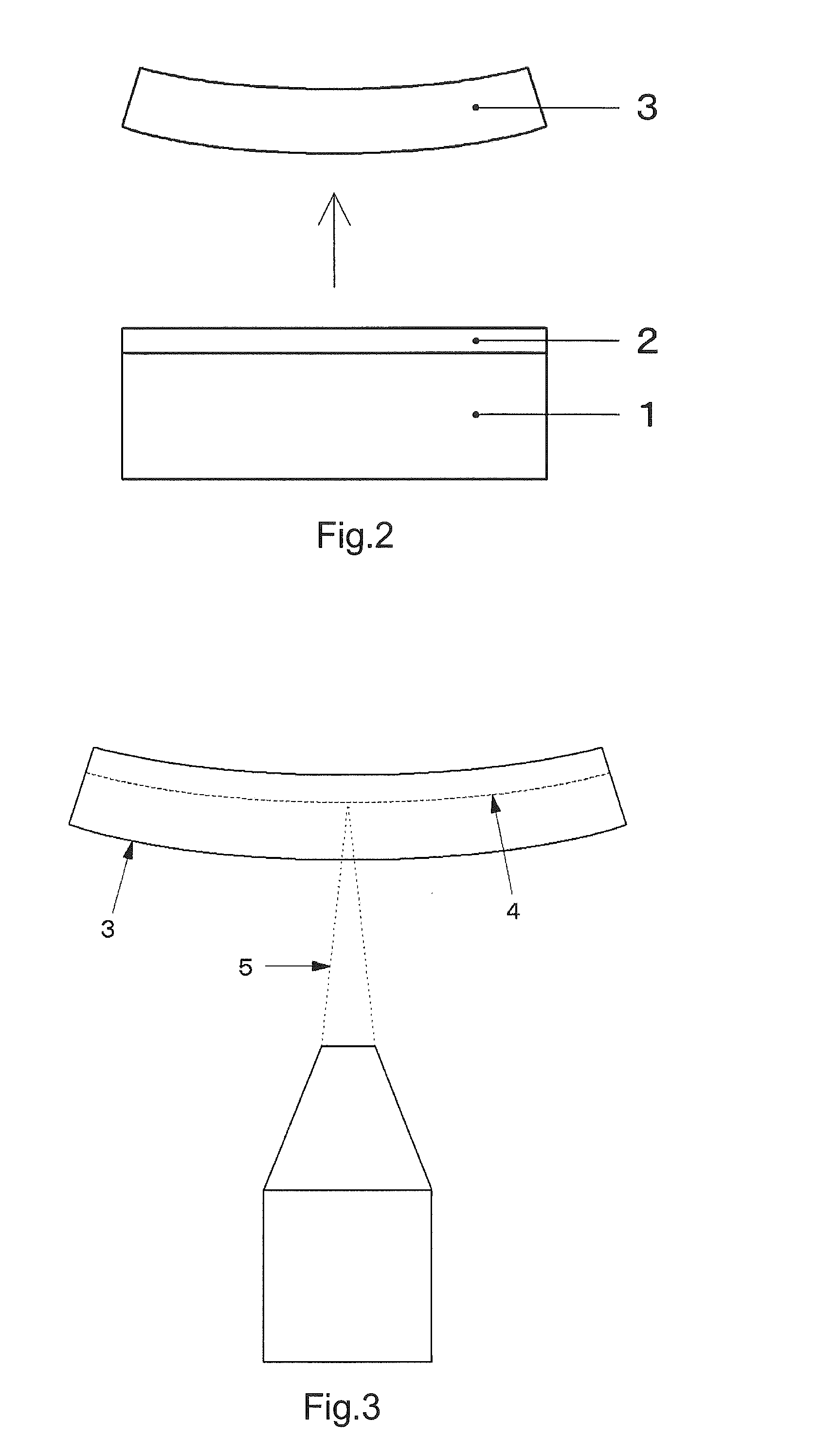
[0060]Hereinbelow, a crystalline film, a device, and manufacturing methods for the crystalline film and the device according to the present invention are described with reference to FIGS. 1 to 4. FIG. 1 are schematic diagrams illustrating epitaxial growth steps for a crystalline film according to an embodiment of the present invention.

[0061]The crystalline film of the present invention has a feature that the crystalline film is formed on a substrate for epitaxial growth (hereinafter, referred to as a “substrate for growth”) so as to have a thickness of 300 μm or more and 10 mm or less by epitaxial growth, is separated from the substrate for growth, and has a reformed region pattern formed in its internal portion.

[0062]On the surface of a crystal growth surface of a substrate for growth 1 illustrated in FIG. 1A, a low-temperature buffer layer 2 is epitaxially grown, as illustrated in FIG. 1B. In addition, as illustrated in FIG. 1C, a crystalline film 3 is formed by epitaxial growth. ...


PUM


Abstract

Provided are a crystalline film in which variations in the crystal axis angle after separation from a substrate for epitaxial growth have been eliminated, and various devices in which the properties thereof have been improved by including the crystalline film. And the crystalline film has a thickness of 300 μm or more and 10 mm or less and reformed region pattern is formed in an internal portion of the crystalline film.

Description

CROSS REFERENCE TO RELATED APPLICATIONS[0001]This is a U.S. national stage of application No. PCT / JP2011 / 055085, filed on 4 Mar. 2011. Priority under 35 U.S.C. §119 (a) and 35 U.S.C. §365(b) is claimed from Japanese Application No. 2010-049860, filed 5 Mar. 2010, the disclosure of which are also incorporated herein by reference.TECHNICAL FIELD[0002]The present invention relates to a crystalline film produced by using a substrate for epitaxial growth, a device, and manufacturing methods for the crystalline film and the device.BACKGROUND ART[0003]A nitride semiconductor represented by gallium nitride (GaN) has a wide band gap and is capable of blue light emission, and hence the nitride semiconductor is widely used in a light emitting diode (LED), a semiconductor laser (LD), and the like. For example, a white LED in which a blue LED containing GaN and a yellow light emitting element are combined is prevalent as a backlight for a liquid crystal display (LCD) of a cellular phone or the l...

Claims


Application Information

Patent Timeline
IPC IPC(8): H01L29/20H01L21/205
CPCH01L21/0237H01L21/02428H01L21/02458C30B33/04H01L21/02686H01L21/02691H01L21/268H01L21/0254H01L21/0242H01L21/20
Inventor AIDA, HIDEOAOTA, NATSUKOHOSHINO, HITOSHIFURUTA, KENJIHAMAMOTO, TOMOSABUROHONJO, KEIJI
Owner NAMIKI SEIMITSU HOSEKI KK
Why Eureka
Try Eureka