Graphical quantum-dot thin film preparation method based on electrostatic induction

An electrostatic induction and thin film preparation technology, which is applied in semiconductor/solid-state device manufacturing, nanotechnology for materials and surface science, circuits, etc., can solve the problems of insufficient precision, affecting the display quality of displays, and low manufacturing costs. The effect of high control precision, simple operation and high efficiency

Inactive Publication Date: 2017-08-18
SOUTH CHINA UNIV OF TECH
View PDF2 Cites 10 Cited by
  • Summary
  • Abstract
  • Description
  • Claims
  • Application Information

AI Technical Summary

Problems solved by technology

The manufacturing cost of printing and photolithography is low, but the pre

Method used


Image

  • Graphical quantum-dot thin film preparation method based on electrostatic induction
  • Graphical quantum-dot thin film preparation method based on electrostatic induction
  • Graphical quantum-dot thin film preparation method based on electrostatic induction

Examples


Embodiment 1

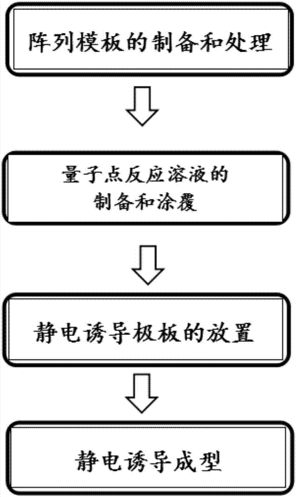
[0046] This embodiment provides a method for preparing a patterned quantum dot film based on electrostatic induction, comprising the following steps:

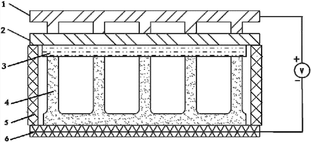
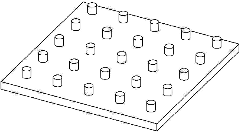
[0047] (1) Preparation and processing of the array template: select a rectangular red copper plate with a size of 50 mm×100 mm and a thickness of 2 mm, and use photolithography and etching processes to process the required micro-column array pattern structure on one surface of the copper plate, as The array template of the electrostatic induction process; the processed micro-pillar array is a cylindrical array, the diameter of the micro-cylindrical bottom of the cylindrical array is 2 μm, the height range of the micro-cylindrical is 4 μm, and the distance between the central axes of the adjacent micro-pillars of the array mold is 5 μm; Electrodes and wires are pasted on the unstructured surface, and connected to the positive pole of the DC power supply.

[0048] (2) Preparation of quantum dot reaction solution: quantum dot reac...

Embodiment 2

[0055] This embodiment provides a method for preparing a patterned quantum dot film based on electrostatic induction, comprising the following steps:

[0056] (1) Preparation and processing of the array template: select a rectangular copper plate with a size of 50mm×100mm and a thickness of 2mm, and use photolithography and etching processes to process the required micro-column array pattern structure on one surface of the copper plate, as The array template of the electrostatic induction process; the processed micro-column array is a square column array, the side length of the bottom surface of the square column array is 0.1 μm, the height of the micro-square column is 1 μm, and the distance between the central axes of the adjacent micro-columns of the array mold is 0.5 μm; paste electrodes and wires on the unstructured surface of the array mold, and connect the positive pole of the DC power supply.

[0057] (2) Preparation of quantum dot reaction solution: quantum dot reacti...

Embodiment 3

[0064] This embodiment provides a method for preparing a patterned quantum dot film based on electrostatic induction, comprising the following steps:

[0065] (1) Preparation and processing of the array template: select a rectangular copper plate with a size of 50mm×100mm and a thickness of 2mm, and use photolithography and etching processes to process the required micro-column array pattern structure on one surface of the copper plate, as The array template of the electrostatic induction process; the processed micro-pillar array is a cylindrical array, the diameter of the micro-cylindrical bottom of the cylindrical array is 10 μm, the height of the micro-square column is 100 μm, and the distance between the central axes of the adjacent micro-pillars of the array mold is 15 μm; Electrodes and wires are pasted on the unstructured surface, and connected to the positive pole of the DC power supply.

[0066] (2) Preparation of quantum dot reaction solution: quantum dot reaction so...


PUM


Abstract

The invention discloses a graphical quantum-dot thin film preparation method based on electrostatic induction. The method comprises the steps of (1) preparation and treatment of an array template; (2) preparation and coating of a quantum-dot reaction solution; (3) placement of electrostatic induction pole plates; and (4) electrostatic induction molding. The method combining electrostatic induction and the microstructural template is adopted, a quantum-dot color film substrate is prepared, the preparation process of quantum dots and the molding process of a quantum dot color film array are combined, and accordingly one-step operation is achieved; and the method is easy to operate, high in efficiency and control precision, suitable for molding of red, green and blue quantum dot color film, problems existing in the prior art are effectively solved, the manufacturing cost is lowered, and the method is suitable for a large-scale production process.

Description

technical field [0001] The invention relates to the field of display technology, in particular to a method for preparing a patterned quantum dot film. [0002] technical background [0003] With the continuous development of display technology, people have higher and higher requirements on display quality of display devices. Quantum Dots (Quantum Dots), as a new type of fluorescent material, has attracted widespread attention. Quantum dot materials refer to semiconductor crystal grains with a particle size of 1-100nm. Compared with traditional fluorescent materials, quantum dot materials can emit high-purity monochromatic light with higher luminous efficiency, so the display color is more vivid, the contrast is high, energy saving and high efficiency are brought about better display effect, and it has unparalleled advantages and potential. Quantum dot materials have received extensive attention, and quantum dot display technology is also rising rapidly. [0004] Compared ...

Claims


Application Information

Patent Timeline
IPC IPC(8): C23C18/12H01L51/00B82Y30/00B82Y40/00B82Y20/00
CPCC23C18/1216C23C18/125B82Y20/00B82Y30/00B82Y40/00H10K71/12
Inventor 李宗涛汤勇余彬海陈钧驰余树东李家声
Owner SOUTH CHINA UNIV OF TECH
Why Eureka
Try Eureka