Film thickness detection device and method

A detection device and a technology for film thickness, which are applied in measurement devices, electromagnetic measurement devices, and electrical devices, etc., can solve problems such as environmental interference of film thickness detection devices

Inactive Publication Date: 2017-08-18
WEIHAI HUALING OPTO ELECTRONICS CO LTD
View PDF8 Cites 2 Cited by
  • Summary
  • Abstract
  • Description
  • Claims
  • Application Information

AI Technical Summary

Problems solved by technology

[0005] Embodiments of the present invention provide a film thickness detection device and method to at least solve the ...

Method used


Image

  • Film thickness detection device and method
  • Film thickness detection device and method
  • Film thickness detection device and method

Examples


Embodiment 1

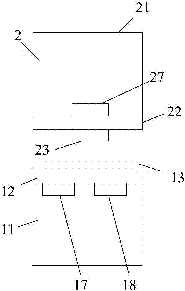
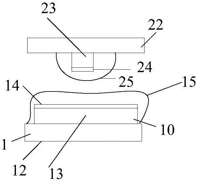
[0029] According to an aspect of an embodiment of the present invention, a film thickness detection device is provided, including: a common electrode, a detection electrode, a common electrode voltage generation circuit, a detection electrode signal processing circuit, the common electrode and the detection electrode are opposite in a first direction and The first common surface of the common electrode is opposite to the first detection surface of the detection electrode, and the detection channel of the film to be tested is formed between the first common surface and the first detection surface, wherein the common electrode voltage generation circuit is used for A voltage is generated on the electrode, so that an effective signal voltage is induced on the detection electrode; the detection electrode signal processing circuit includes: a reset voltage timing control circuit, a detection electrode effective signal voltage transfer timing control circuit and a differential amplifi...

Embodiment 2

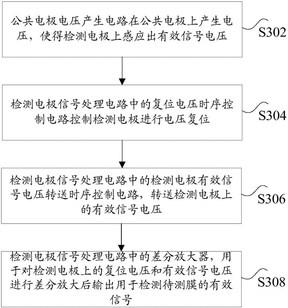
[0044] According to another embodiment of the present invention, a method embodiment of a film thickness detection method is also provided. It should be noted that the steps shown in the flow chart of the accompanying drawings can be implemented in a computer system such as a set of computer-executable instructions and, although the logic sequence is shown in the flow chart, in some cases, the steps shown or described can be executed in a different order than here, and the film thickness detection method of the embodiment of the present invention can be used To implement the film thickness detection device provided by the embodiment of the present invention. The film thickness detection method provided by the embodiment of the present invention is introduced below.

[0045] In this embodiment, a film thickness detection method is provided, image 3 The flowchart of the film thickness detection method according to the embodiment of the present invention, such as image 3 As s...


PUM


Abstract

The invention discloses a film thickness detection device and method. The device comprises common electrodes, detection electrodes, a common electrode voltage generation circuit and a detection electrode signal processing circuit. A detection channel for a film to be detected is formed between a first common surface and a first detection surface. The common electrode voltage generation circuit is used for generating voltage on the common electrodes so that effective signal voltage is enabled to be induced on the detection electrodes. The detection electrode signal processing circuit comprises a reset voltage sequence control circuit, a detection electrode effective signal voltage transmission sequence control circuit and a differential amplifier. The reset voltage sequence control circuit is used for controlling the detection electrodes to perform voltage resetting. The detection electrode effective signal voltage transmission sequence control circuit is used for transmitting the effective signal voltage on the detection electrodes. The differential amplifier is used for performing differential amplification on the reset voltage and the effective signal voltage on the detection electrodes and then outputting effective signals used for detecting the film to be detected.

Description

technical field [0001] The invention relates to the field of digital detection, in particular to a film thickness detection device and method. Background technique [0002] As we all know, the online continuous thickness measurement of sheet-like items, such as paper, bills, plastic films, and textile items, plays an increasingly important role in the production, testing, processing, and recycling of corresponding products. In recent years, the detection technology of film thickness through electrostatic induction between electrodes has been continuously researched and explored. For example, a capacitive paper thickness sensor in the related art mainly converts the capacitance change of the capacitor into the change of the oscillation frequency. The frequency change is then converted into a voltage change by the frequency-voltage conversion module. In addition, a material thickness detection method in the related art mainly uses the plate of the plate capacitor as a sensiti...

Claims


Application Information

Patent Timeline
IPC IPC(8): G01B7/06
CPCG01B7/06G01B7/085G07D7/026G07D7/164G01R19/0084H03K17/22G01B7/087
Inventor 姜利林永辉祁秀梅孙明丰
Owner WEIHAI HUALING OPTO ELECTRONICS CO LTD
Why Eureka
Try Eureka