A kind of dual voltage domain driving operation circuit

An arithmetic circuit and dual-voltage technology, applied in transducer circuits, electrical components, signal processing, etc., can solve problems such as insufficient open-loop gain, increased chip cost, and increased design difficulty, achieving simple structure, large opening Loop gain, avoiding the effect of complex structure of op amp

Active Publication Date: 2020-01-03
BUILDWIN SEMICON SHENZHEN CO LTD
View PDF6 Cites 0 Cited by
  • Summary
  • Abstract
  • Description
  • Claims
  • Application Information

AI Technical Summary

Problems solved by technology

The 1.2V voltage domain drive circuit also needs to consider the problem of insufficient open-loop gain, which undoubtedly increases the difficulty of design
At the same time, two high-power output op amps will occupy the layout area of ​​the two op amps, increasing the cost of the chip

Method used


Image

  • A kind of dual voltage domain driving operation circuit
  • A kind of dual voltage domain driving operation circuit

Examples


Embodiment 1

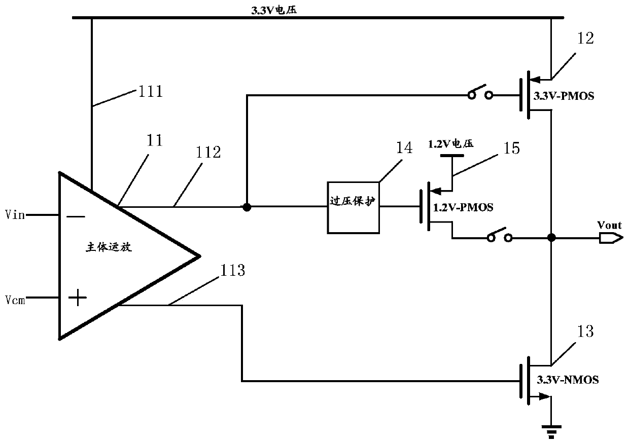
[0022] refer to figure 1 , a dual voltage domain drive operation circuit provided in the embodiment of the present application, including: a main operational amplifier 11, a 3.3V-PMOS transistor 12, a 3.3V-NMOS transistor 13, an overvoltage protection circuit 14, a 1.2V-PMOS transistor 15 and Output terminal Vout.

[0023] Wherein, the main operational amplifier 11 further includes: a non-inverting input terminal Vcm, an inverting input terminal Vin, a power input terminal 111 , a first output terminal 112 , and a second output terminal 113 .

[0024] The non-inverting input terminal Vcm and the inverting input terminal Vin of the main operational amplifier 11 are respectively used for connecting input signals. The first output terminal 112 is connected to the overvoltage protection circuit 14 and connected to the gate of the 3.3V-PMOS transistor 12 through a switch. The second output terminal 113 is connected to the gate of the 3.3V-NMOS transistor 13 . The power input ter...

Embodiment 2

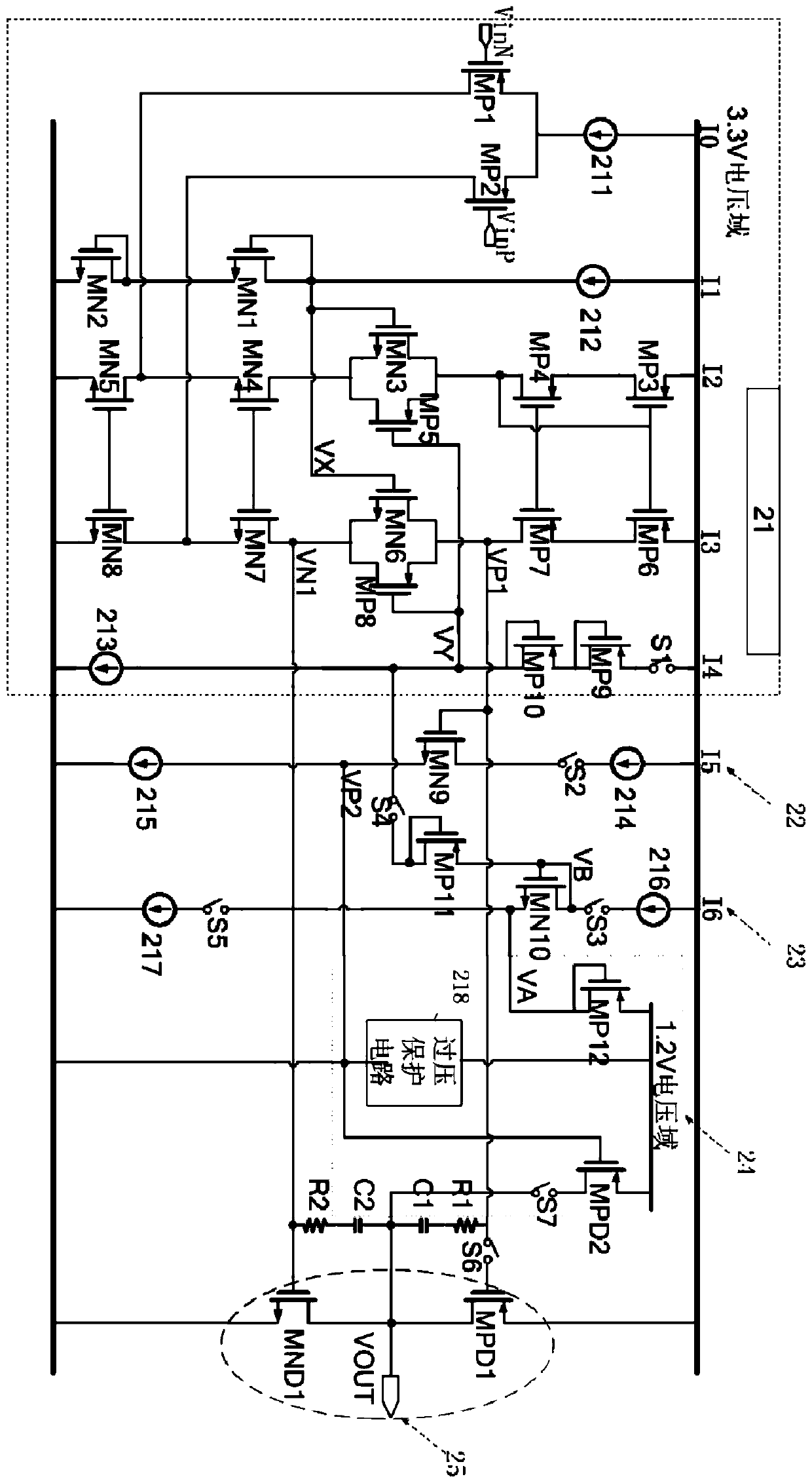
[0031] On the basis of the first embodiment, a dual voltage domain driving operation circuit is further described.

[0032] refer to figure 2 , a specific structural diagram of a dual voltage domain driving operation circuit in the second embodiment.

[0033] The circuit includes a main operational amplifier 21 , a translation circuit 22 , a 1.2v output stage static bias circuit 23 and a 1.2v voltage domain circuit 24 .

[0034] Specifically, the main operational amplifier circuit 21 includes: a branch circuit I0 , a branch circuit I1 , a branch circuit I2 , a branch circuit I3 and a branch circuit I4 .

[0035] Wherein, the branch circuit I0 includes: a first current source 211 , a PMOS transistor MP1 and a PMOS transistor MP2 , wherein the sources of the PMOS transistor MP1 and the PMOS transistor MP2 are connected to a 3.3v power supply through the first current source 211 . The gate of the PMOS transistor MP1 is used as an inverting input terminal VinN, and the gate of ...

Embodiment 3

[0068] Embodiment 3 of the present application provides an electronic device, including the dual-voltage-domain driving operation circuit described in Embodiment 1 and Embodiment 2 above.


PUM


Abstract

The embodiment of the invention discloses a dual-voltage domain driving operation circuit. The operation circuit comprises a main body operational amplifier, a first output PMOS tube, a first output NMOS tube, an over-voltage protecting circuit, and a second output PMOS tube, wherein the main body operational amplifier comprises a noninverting input end, an inverting input end, a first output end and a second output end, wherein the noninverting input end and the inverting input end of the main body operational amplifier are respectively used for connecting an input signal; the first output end is connected with a grid of the first output PMOS tube or the first output end is connected with the grid of the second output PMOS through an over-voltage protecting circuit; the second output end is connected with the grid of the first output NMOS tube. Two voltage domain output stages in the invention share the NMOS tube, the 3.3V mode output stage adopts the 3.3V PMOS and 3.3V NMOS to construct the output stage; the 1.2V mode output stage adopts the 1.2V PMOS tube and 3.3V NMOS tube to form the output stage. The sharing of the output stage NMOS tube can further save the layout area.

Description

technical field [0001] The embodiments of the present invention relate to the technical field of integrated circuits, in particular to a dual-voltage domain driving operation circuit. Background technique [0002] With the development of SOC chips, the market has higher and higher requirements for chips, and the chip itself will have more and more functions. For example, the headphone drive circuit in the chip, the usual chip is designed with 3.3V MOS headphone drive circuit. In order to achieve a large output range, the general headphone load is only 32 ohms or 16 ohms, and the headphone drive circuit will draw a large current from the power supply when driving the headphones. But with the rise of portable devices, low-voltage low-power devices will become mainstream (Bluetooth headsets, etc.). The 1.2V power supply circuit can effectively reduce system power consumption and prolong the use time of portable devices. In order to expand the functions of the chip and expand ...

Claims


Application Information

Patent Timeline
Patent Type & Authority Patents(China)
IPC IPC(8): H04R3/00
CPCH04R3/00H04R2430/00
Inventor 陈昊
Owner BUILDWIN SEMICON SHENZHEN CO LTD
Why Eureka
Try Eureka