Composite magnetic field sensor and manufacturing process thereof

A composite magnetic field and manufacturing process technology, applied in the field of magnetic field sensors, can solve problems such as the inability to detect a wide range of magnetic fields

Active Publication Date: 2017-08-25
HEILONGJIANG UNIV
View PDF8 Cites 2 Cited by
  • Summary
  • Abstract
  • Description
  • Claims
  • Application Information

AI Technical Summary

Problems solved by technology

However, the magnetotransistor is used to detect a strong magnetic field, and the general detection range is 500 ~ 10000G S Above, the tunneling magneto-resistor (TMR) is used to detect weak magnetic fields, and its general detection range is 1G S Below, however, when applied, the detected magnetic field is not necessarily a strong magnetic field or a weak magnetic field, but a wide range of magnetic field strengths, and the wide-range magnetic field cannot be detected according to the prior art

Method used


Image

  • Composite magnetic field sensor and manufacturing process thereof
  • Composite magnetic field sensor and manufacturing process thereof
  • Composite magnetic field sensor and manufacturing process thereof

Examples


Embodiment approach

[0067] According to a preferred embodiment of the present invention, the magnetotransistor is a silicon magnetotransistor (SMST).

[0068] In a further preferred embodiment, the magnetotransistor is an NPN silicon magnetotransistor.

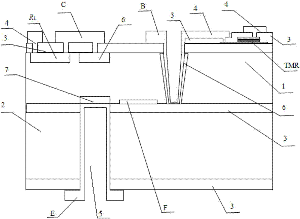
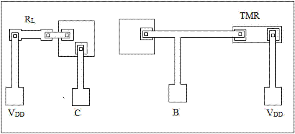
[0069] According to a preferred embodiment of the present invention, such as figure 1 As shown, the magnetotransistor includes a first silicon chip 1 and a second silicon chip 2 .

[0070] In a further preferred embodiment, the first silicon wafer 1 and the second silicon wafer 2 are both oriented high-resistance p-type single crystal silicon wafers.

[0071] In a further preferred embodiment, the thickness of the first silicon wafer 1 is 30 μm, and the thickness of the second silicon wafer is 400-425 μm.

[0072] According to a preferred embodiment of the present invention, such as figure 1 As shown, an emitter region is etched on the lower surface of the first silicon chip 1, and an Al lead 4 is etched on the emitter region to form an emitt...

experiment example 1

[0128] Experimental example 1 Composite sensor characteristic test

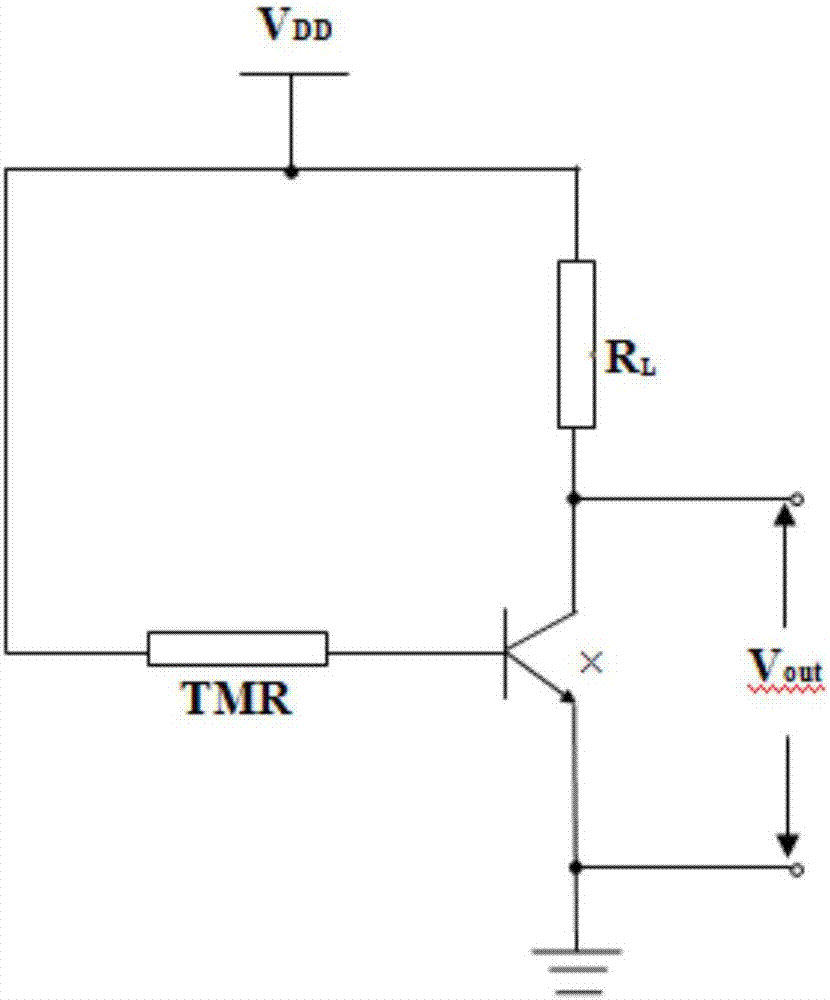
[0129] The composite sensor was tested with the zero-magnetic shielding magnetic field generation system of Beijing Cuihai Jiacheng Magnetic Technology Co., Ltd., and the magnetic field detection sensitivity of the composite sensor was analyzed. After testing, it can be known that the composite magnetic sensor can successfully detect 0.001G S ~10000G S The magnetic induction intensity between.


PUM

PropertyMeasurementUnit
Thicknessaaaaaaaaaa
Thicknessaaaaaaaaaa
Depthaaaaaaaaaa

Abstract

The invention discloses a composite magnetic field sensor and a manufacturing process thereof. The composite magnetic field sensor comprises a magnetic sensitive transistor and a tunneling magnetic resistor (TMR) composited on the magnetic sensitive transistor. The collector region of the magnetic sensitive transistor is arranged above the emitter region. The base region is arranged at one side of the emitter region and the collector region, and is manufactured in a silicon corrosion pit. The carrier injection ability of the base region is improved, and the magnetic sensitivity of the magnetic sensitive transistor is improved. The composite magnetic field sensor is prepared by combining the manufacturing process with a microelectronic mechanical system (MEMS) technology, a bipolar process and a nano film preparation technology. The composite magnetic field sensor combining the magnetic sensitive transistor and the tunneling magnetic resistor has both the strong magnetic field detection performance of the magnetic sensitive transistor and the weak magnetic field detection performance of the tunneling magnetic resistor. Thus, wide-range magnetic field detection is realized.

Description

technical field [0001] The invention relates to a magnetic field sensor, in particular to a magnetic field sensor with a wide range, in particular to a composite magnetic field sensor with a wide range and a manufacturing process thereof. Background technique [0002] With the rapid development of science and technology, sensor technology has attracted much attention, especially the magnetic field sensors that are widely used in modern industry and electronic products. With the wide application, the requirements for the measurement range of magnetic field sensors have also increased. [0003] In the prior art, sensors for detecting magnetic fields include magnetotransistors, anisotropic magnetoresistance (AMR), giant magnetoresistance (GMR), tunneling magnetoresistance (TMR), and Hall magnetic field sensors. However, the magnetosensitive triode is used to detect a strong magnetic field, and the general detection range is 500 ~ 10000G S Above, the tunneling magneto-resistor ...

Claims


Application Information

Patent Timeline
IPC IPC(8): G01R33/06G01R33/09G01R33/00H01L43/08
CPCG01R33/0005G01R33/0052G01R33/06G01R33/098H10N50/10Y02P70/50
Inventor 赵晓锋邓祁艾春鹏温殿忠
Owner HEILONGJIANG UNIV
Why Eureka
Try Eureka