A bismuth iodide two-dimensional material, its preparation and application

A two-dimensional material, bismuth iodide technology, applied in the field of nanomaterials, can solve problems such as poor crystallinity, poor morphology, and nanosheet thickness, and achieve the effect of improving performance

Active Publication Date: 2019-12-24
HUNAN UNIV
View PDF1 Cites 0 Cited by
  • Summary
  • Abstract
  • Description
  • Claims
  • Application Information

AI Technical Summary

Problems solved by technology

[0015] An object of the present invention is to solve technical problems such as thickness of nanosheets, uneven appearance, poor crystallinity, and poor appearance in existing preparation methods. The present invention provides a preparation method of a bismuth iodide two-dimensional material, Bismuth iodide nanosheets and bismuth iodide heterojunction products can be prepared by replacing the substrate

Method used


Image

  • A bismuth iodide two-dimensional material, its preparation and application
  • A bismuth iodide two-dimensional material, its preparation and application
  • A bismuth iodide two-dimensional material, its preparation and application

Examples


Embodiment 1

[0080] Preparation of bismuth iodide nanosheets:

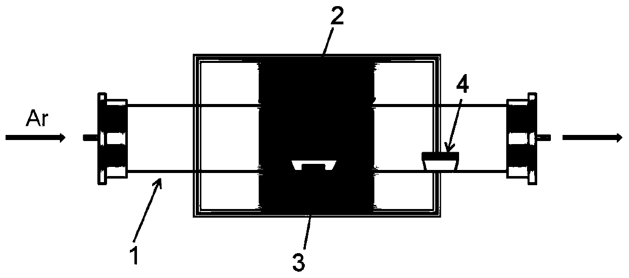
[0081] Put the porcelain boat containing 0.1g of bismuth iodide powder in the constant temperature zone of the tube furnace, and a piece of Si / 300nmSiO 2 as BiI 3 The bright side of the growth substrate is placed on another porcelain boat and placed in the variable temperature zone downstream of the furnace to obtain an appropriate crystal growth temperature. Before heating, exhaust the air in the quartz tube with a large flow of argon. Then the furnace is heated up to 305° C., and the argon gas flow rate is 225 sccm, and the temperature is kept constant for 15 minutes, and single crystal bismuth iodide nanosheets will be formed on a certain position of the silicon wafer. The experimental setup of bismuth iodide nanosheets is shown in Fig. figure 1 As shown, the optical photographs of the prepared bismuth iodide nanosheets are as follows image 3 shown.

[0082] image 3 The optical schematic diagram of the prepared bis...

Embodiment 2

[0084] Preparation of bismuth iodide nanosheets:

[0085] Put the porcelain boat containing 0.1g of bismuth iodide powder in the constant temperature zone of the tube furnace, and a piece of Si / 300nmSiO 2 as BiI 3 The bright side of the growth substrate is placed on another porcelain boat and placed in the variable temperature zone downstream of the furnace to obtain an appropriate crystal growth temperature. Before heating, exhaust the air in the quartz tube with a large flow of argon. Then the furnace is heated up to 310° C., and the argon gas flow rate is 100 sccm, and the temperature is kept constant for 10 minutes. Single crystal bismuth iodide nanosheets will be formed on a certain position of the silicon wafer. The experimental setup of bismuth iodide nanosheets is shown in Fig. figure 1 As shown, the optical photographs of the prepared bismuth iodide nanosheets are as follows Figure 4 shown.

[0086] Figure 4 The optical schematic diagram of the prepared bismu...

Embodiment 3

[0088] Compared with Example 1, the difference lies in that the growth temperature is 310° C., the flow rate is 225 sccm, and the deposition time is 13 minutes. Figure 5 The optical schematic diagram of the prepared bismuth iodide nanosheets, the Si / SiO2 substrate is purple, and the white, blue and gray hexagons are bismuth iodide. Figure 5 The scale bar in is 5 μm.


PUM

PropertyMeasurementUnit
thicknessaaaaaaaaaa
thicknessaaaaaaaaaa
thicknessaaaaaaaaaa

Abstract

The invention relates to a preparation method of a bismuth iodide two-dimensional material and electrical and optoelectronic devices made of the material. A novel bismuth iodide nanosheet two-dimensional material is obtained through expansion. The preparation of a vertical heterojunction and electrical and optoelectronic devices offers new possibilities for the discovery of novel electrical and optoelectronic device equipment. The method comprises the following steps: placing a porcelain boat containing bismuth iodide powder in a constant temperature zone of a single-temperature-zone tubular furnace; setting the temperature of the constant temperature zone to 305-360 DEG C; taking empty Si / 300nmSiO2 and Si / 300nmSiO2 with WSe2 / WS2 nanosheets grown thereon as a growth substrate of the two-dimensional material, and placing the Si / 300nmSiO2 in a variable temperature zone or room temperature zone on the downstream of the furnace; setting the flow rate of carrier gas (argon) to 5-225sccm; and obtaining a bismuth iodide two-dimensional material through fast growth at constant temperature for 10-15min or by moving a silicon wafer through a magnet. The BiI3 two-dimensional material is prepared by depositing Cr (20nm) and Au (80nm) through electron beam lithography. The bismuth iodide nanosheet prepared using the method has a good hexagonal shape, has thickness of 10-120nm, is 3-10 microns in size, is monocrystal, and is of high quality. The hetero junction preparation method is simple and feasible.

Description

technical field [0001] The invention belongs to the field of nanometer materials, and specifically relates to bismuth iodide two-dimensional materials, preparation and application in electrical and optoelectronic devices. [0002] technical background [0003] Bismuth iodide is a layered material. [0004] The discovery of graphene has triggered a research boom in the scientific community on two-dimensional layered materials, especially for the exploration of MoS 2 New physical and chemical properties of the representative two-dimensional transition metal dichalcogenides (2D-TMDs) at the atomic level [1-2] . The interlayer forces of 2D transitional metal dichalcogenides are van der Waals forces, making 2D-TMDs easily exfoliated into monolayers or few layers, and form van der Waals heterogeneity with other 2D materials without requiring lattice matching structure (vdWHs). Recent studies have reported many practical applications of 2D-TMDs and vdWHs, including atomic-thick ...

Claims


Application Information

Patent Timeline
Patent Type & Authority Patents(China)
IPC IPC(8): H01L21/34H01L29/24H01L29/78B82Y30/00B82Y40/00
CPCB82Y30/00B82Y40/00H01L21/34H01L29/24H01L29/66969H01L29/7827
Inventor 段镶锋段曦东李佳
Owner HUNAN UNIV
Why Eureka
Try Eureka