Array substrate, manufacturing method thereof and display device

The technology of an array substrate and its manufacturing method, which is applied in the field of display, can solve the problems of high light reflectance of the light-shielding layer, the unsteady use of the array substrate, and the shift of the threshold voltage of the thin-film transistor, so as to achieve the effect of improving the stability of use

Active Publication Date: 2017-08-25
BOE TECH GRP CO LTD
View PDF5 Cites 12 Cited by
  • Summary
  • Abstract
  • Description
  • Claims
  • Application Information

AI Technical Summary

Problems solved by technology

[0004] However, because the existing light-shielding layer is generally made of metal materials, such as molybdenum (Mo) metal, etc., the light-shielding layer has a high light reflectivity.
Therefore, if there is external light, or reflected light from other functional film layers, and irradiates the surface of the light-shielding layer facing the active layer, the light-s

Method used


Image

  • Array substrate, manufacturing method thereof and display device
  • Array substrate, manufacturing method thereof and display device
  • Array substrate, manufacturing method thereof and display device

Examples


Embodiment Construction

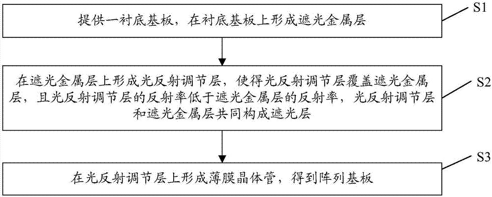
[0029] In order to further illustrate the array substrate, its manufacturing method, and display device provided by the embodiments of the present invention, a detailed description will be given below in conjunction with the accompanying drawings.

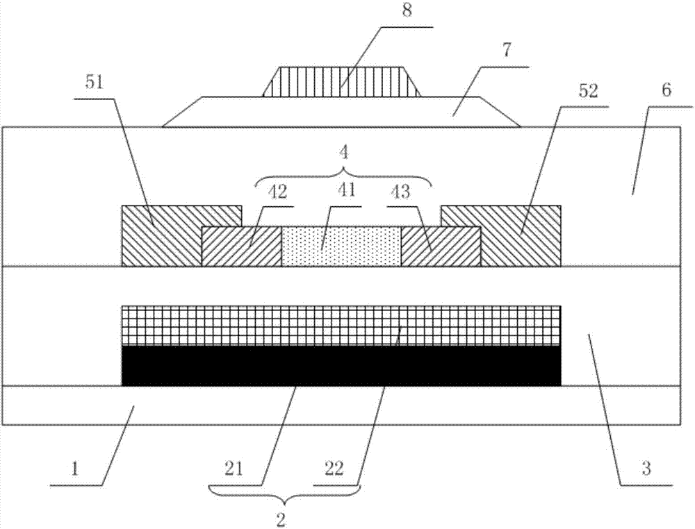
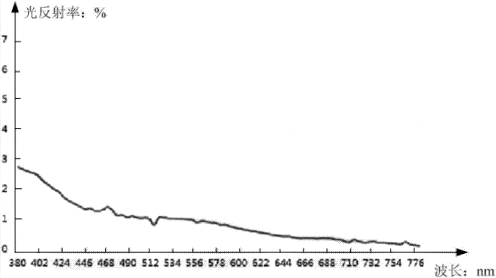
[0030] see figure 1 The array substrate provided by the embodiment of the present invention includes a base substrate 1 and a thin film transistor disposed on the base substrate 1; a light-shielding layer 2 is arranged between the thin-film transistor and the base substrate 1, and the light-shielding layer 2 includes layers formed on the base substrate 1, the light-shielding metal layer 21 and the light reflection adjustment layer 22, the light reflection adjustment layer 22 covers the light-shielding metal layer 21, and the reflectance of the light reflection adjustment layer 22 is lower than the reflectance of the light-shielding metal layer 21.

[0031] During specific implementation, in the array substrate provided by the embod...


PUM


Abstract

The invention discloses an array substrate, a manufacturing method thereof and a display device, which relate to the technical field of display and aim at improving the use stability of the array substrate. The array substrate comprises a substrate and a thin-film transistor arranged on the substrate, wherein a light shielding layer is arranged between the thin-film transistor and the substrate; the light shielding layer comprises a light shielding metal layer and a light reflection adjustment layer formed on the substrate in a stacked mode; the light reflection adjustment layer covers the light shielding metal layer; and the reflectivity of the light reflection adjustment layer is lower than that of the light shielding metal layer. According to the array substrate, the manufacturing method thereof and the display device provided by the invention, the array substrate adopts the thin-film transistor in a top gate structure.

Description

technical field [0001] The present invention relates to the field of display technology, in particular to an array substrate, a manufacturing method thereof, and a display device. Background technique [0002] A thin film transistor (Thin Film Transistor, TFT for short), as a switching device, plays an important role in the field of display technology. Common thin film transistors include a gate, source, drain, and active layer, etc., and according to the relative positional relationship between the gate and the active layer, thin film transistors can be divided into thin film transistors with a top-gate structure and bottom-gate structures. structure of thin film transistors. [0003] At present, when a thin-film transistor with a top-gate structure is arranged on an array substrate, the active layer of the thin-film transistor is located between its gate and the base substrate of the array substrate, and a light-shielding layer is usually provided between the active layer...

Claims


Application Information

Patent Timeline
IPC IPC(8): H01L27/12H01L23/552H01L21/77
CPCH01L23/552H01L27/1214H01L27/1259H01L29/78633H01L27/1222H01L27/1251H01L27/127
Inventor 张斌詹裕程周婷婷何晓龙
Owner BOE TECH GRP CO LTD
Why Eureka
Try Eureka