Supercharge Your Innovation With Domain-Expert AI Agents!

Method for writing in an EEPROM memory and corresponding device

A technology for writing operations and memory cells, which is applied in the field of memory, and can solve problems such as unacceptable number of write times, write problem obstacles, etc.

Active Publication Date: 2017-08-29
STMICROELECTRONICS SRL
View PDF3 Cites 2 Cited by
  • Summary
  • Abstract
  • Description
  • Claims
  • Application Information

AI Technical Summary

Problems solved by technology

[0011] There is a limit to increasing the duration of the applied erase and program pulses, as this would result in unacceptable write cycles
[0012] Therefore, especially for non-volatile memories of the EEPROM type, the problem of writing poses an obstacle to the development of its modern technology
[0013] Furthermore, there is a need for low power for memory operations, thus limiting the value of the realized voltages, especially for autonomous systems such as hearing aids with small batteries, or for radio frequency identification "RFID" tags

Method used


Image

  • Method for writing in an EEPROM memory and corresponding device
  • Method for writing in an EEPROM memory and corresponding device
  • Method for writing in an EEPROM memory and corresponding device

Examples


Embodiment Construction

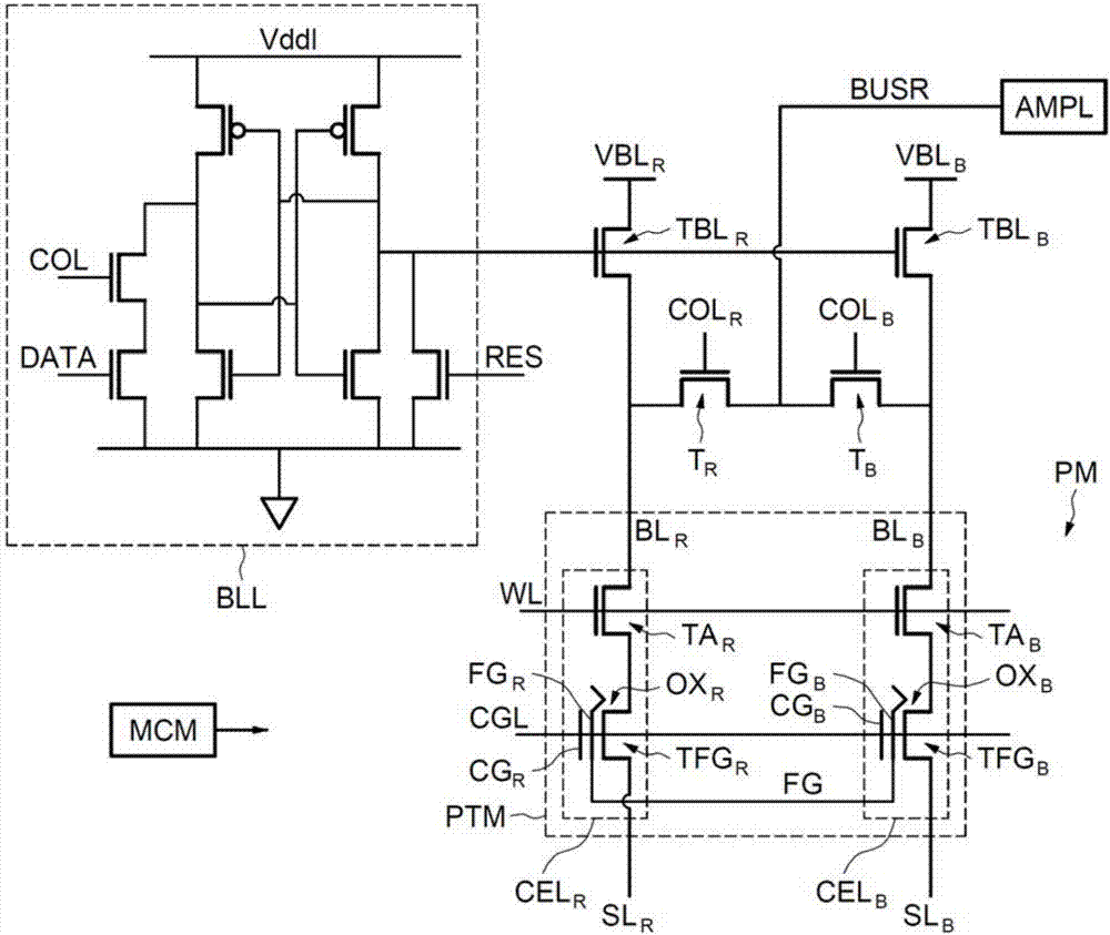
[0049] figure 1 An embodiment of a memory device of the EEPROM type is shown, comprising: a memory location PTM on a memory plane PM; BUSR is in particular a switching element connecting the memory plane PM with the sense amplifier AMPL.

[0050] In particular, the sense amplifier AMPL is configured for reading the content of the bits stored in the memory location PTM.

[0051] Memory location PTM includes two identical memory cells CEL R 、CEL B . first memory cell CEL R is referred to as a "regular cell", while the second memory cell CEL B Known as a "boost unit".

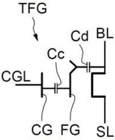
[0052] Conventional memory cell CEL R includes a first-state transistor TFG called “regular” R and the first access transistor TA controlled by a signal passed through the word line WL R , the first access transistor TA R The drain is connected to the first bit line BL R . The first access transistor TA R The source is connected to the first state transistor TFG R the drain.

[0053] First state tr...


PUM


Abstract

The application relates to a method for writing in an EEPROM memory and a corresponding device. A method for writing in a memory location includes at least one operation used for writing a data value, and the operation includes an erasing and / or programming step using a tunnel effect. The memory location includes a first memory cell with a first transistor having a first oxide underlying a first floating gate and a second memory cell with a second transistor having a second oxide underlying a second floating gate that is connected to the first floating gate. The erasing and / or programming step includes a first phase and a second phase, in a first phase, an identical tunnel effect is implemented through each of the oxides, and in a second phase, a voltage across terminals of one of the first oxide and the second oxide is increased and at the same time, a voltage across terminals of the other oxide of the other transistor of the other memory cell is reduced.

Description

technical field [0001] Embodiments of the present invention and implementations thereof relate to memories, particularly electrically erasable programmable (EEPROM) type non-volatile memories, and more particularly to the operation of writing data to these memories. Background technique [0002] In EEPROM memory, the logical value of a bit stored in a memory location is represented by the value of the threshold voltage of a floating gate transistor, which can be arbitrarily modified by a write operation. A write operation generally includes an erase step followed by a programming step. [0003] However, in some cases, a write operation may include only an erase step or only a program step. So, for example, only an erase step is required if the word to be written contains only "0". The erase step is unnecessary if the previous content of the memory location where the digital word needs to be written already contains only "0". [0004] Programming or erasing a floating gate...

Claims


Application Information

Patent Timeline
IPC IPC(8): G11C16/10G11C16/14
CPCG11C16/10G11C16/14G11C16/0441H10B41/30H10B41/40G11C16/0408H01L29/7883
Inventor F·塔耶特
Owner STMICROELECTRONICS SRL
Features
  • R&D
  • Intellectual Property
  • Life Sciences
  • Materials
  • Tech Scout
  • Unparalleled Data Quality
  • Higher Quality Content
  • 60% Fewer Hallucinations
Learn More