Semiconductor device

A semiconductor, n-type technology, applied in the direction of semiconductor devices, transistors, electric solid devices, etc., can solve the problem of concentration reduction in the anode region

Inactive Publication Date: 2017-08-29
MITSUBISHI ELECTRIC CORP
View PDF5 Cites 2 Cited by
  • Summary
  • Abstract
  • Description
  • Claims
  • Application Information

AI Technical Summary

Problems solved by technology

Therefore, the concentration in the anodic region decreases

Method used


Image

  • Semiconductor device
  • Semiconductor device
  • Semiconductor device

Examples


Embodiment approach 1

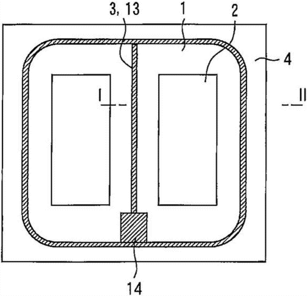
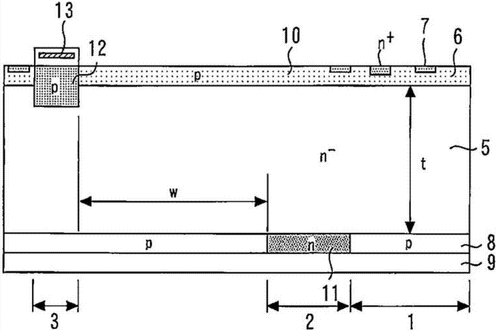
[0024] figure 1 It is a plan view showing the semiconductor device according to Embodiment 1 of the present invention. figure 2 is along figure 1 Sectional view of I-II. This semiconductor device is an RC-IGBT in which IGBT (Insulated Gate Bipolar Transistor) 1 and FWD (Free Wheeling Diode) 2 are formed on one semiconductor substrate. In addition, in the RC-IGBT, there is a wiring region 3 in addition to regions where the IGBT 1 and the FWD 2 operate, and a termination region 4 exists on the periphery of these regions.

[0025] IGBT 1 has: n - Type drift layer 5; p-type base layer 6 and n + type emitter layer 7, they are formed in n - the surface of the drift layer 5; and the p-type collector layer 8, which is formed on the n - type drift layer 5 on the back side. Collector electrode 9 is connected to p-type collector layer 8 . In the MOS structure on the surface side of the IGBT 1, by applying a voltage to the gate, electrons are supplied to the n - Type drift layer...

Embodiment approach 2

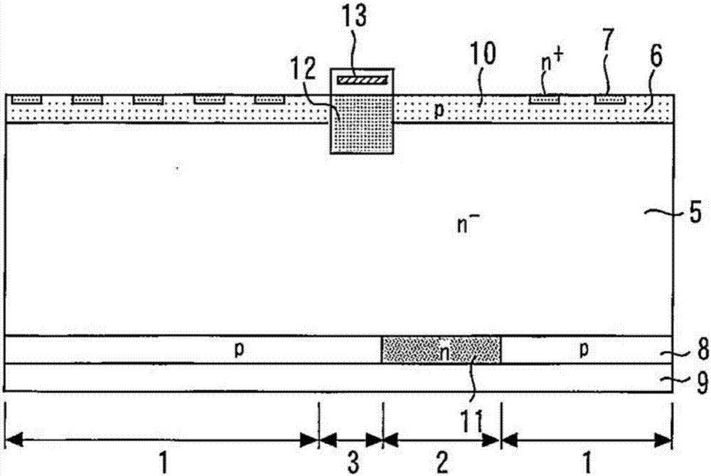
[0034] Figure 4 It is a plan view showing the semiconductor device according to Embodiment 2 of the present invention. Figure 5 is along Figure 4Sectional view of I-II. A plurality of trench gates 15 are formed. The IGBT 1 is formed in a region between the wiring region 3 and the termination region 4 and the FWD 2 . By forming the IGBT 1 in the vicinity of the wiring region 3 and the terminal region 4, the recovery loss of the FWD 2 can be reduced without reducing the effective area of ​​the element (the total area of ​​the IGBT 1 and the FWD 2 that can conduct electricity).

Embodiment approach 3

[0036] Figure 6 It is a plan view showing the semiconductor device according to Embodiment 3 of the present invention. IGBT 1 and FWD 2 are repeatedly formed at constant intervals in a region surrounded by gate wiring 13 in plan view. IGBT 1 and FWD 2 inside the RC-IGBT generate heat due to the flow of current. The maximum rated temperature of the element is usually 150 to 175°C. In order to lower the temperature of the heat-generating element, it is necessary to cool the heat dissipation fins in contact with the back side of the RC-IGBT by air cooling or water cooling. In a normal usage method, the period during which the current flows through the IGBT 1 and the period during which the current flows through the FWD 2 are alternated, and the timings at which the temperatures of the IGBT 1 and the FWD 2 reach peak values ​​are shifted. Therefore, by repeatedly forming IGBT 1 and FWD 2 at fixed intervals, the heat generated when one of IGBT 1 and FWD 2 is energized can also b...


PUM


Abstract

An IGBT 1 has: an n type drift layer 5; a p type base layer 6 and an n type emitter layer 7, which are formed on the front surface of the n type drift layer 5; and a p type collector layer 8 formed on the rear surface of the n type drift layer 5. An FWD 2 has: the n type drift layer 5; a p type anode layer 10 formed on the front surface of the n type drift layer 5; and an n type cathode layer 11 formed on the rear surface of the n- type drift layer 5. In a wiring region 3 and a terminal region 4, a p type well 12 is formed in the front surface of the n- type drift layer 5. In the wiring region 3, wiring 13 is formed on the p type well 12. The p type well 12 has a higher impurity concentration and more depth compared with the p type anode layer 10. The p type well 12 is not formed directly above the n type cathode layer 11, and is separated from a region directly above the n type cathode layer 11.

Description

technical field [0001] The present invention relates to a reverse conducting IGBT (RC (Reverse Conducting)-IGBT) in which a FWD (Free Wheeling Diode) is incorporated in an IGBT (Insulated Gate Bipolar Transistor). Background technique [0002] The losses of IGBTs and FWDs installed in inverters and converters are decreasing year by year. Along with this, the current density of the chip increases and the chip size shrinks. However, in recent years, the losses of IGBTs and FWDs are approaching the limit value. In order to greatly reduce the chip size, the development of power devices made of SiC and RC-IGBTs that combine the performance of IGBTs and FWDs, etc., are still being developed. [0003] Power devices made of SiC can be used at high temperatures, and their losses are expected to be greatly reduced. However, there are issues such as expensive SiC wafer materials and failures due to defects in SiC, and it will take some time before they are widely used in the market. ...

Claims


Application Information

Patent Timeline
Patent Type & Authority Applications(China)
IPC IPC(8): H01L27/04H01L29/739H01L29/78
CPCH01L27/0207H01L27/0727H01L29/7397H01L29/0615H01L29/0834H01L29/1095H01L29/4238H01L29/7395H01L29/861H01L27/0716H01L29/1004
Inventor 春口秀树友松佳史
Owner MITSUBISHI ELECTRIC CORP
Why Eureka
Try Eureka