A thin film transistor and its manufacturing method, a display panel, and a display device

A technology for thin film transistors and display panels, applied in transistors, semiconductor/solid-state device manufacturing, semiconductor devices, etc., to reduce the risk of open circuits, improve product yield, and simplify process flow

Active Publication Date: 2020-06-05
BOE TECH GRP CO LTD +1
View PDF3 Cites 0 Cited by
  • Summary
  • Abstract
  • Description
  • Claims
  • Application Information

AI Technical Summary

Problems solved by technology

[0004] The invention provides a thin film transistor and its manufacturing method, a display panel, and a display device to solve the problem of how to simplify the process flow of a double-gate thin film transistor and improve the yield rate of the product

Method used


Image

  • A thin film transistor and its manufacturing method, a display panel, and a display device
  • A thin film transistor and its manufacturing method, a display panel, and a display device
  • A thin film transistor and its manufacturing method, a display panel, and a display device

Examples


Embodiment 1

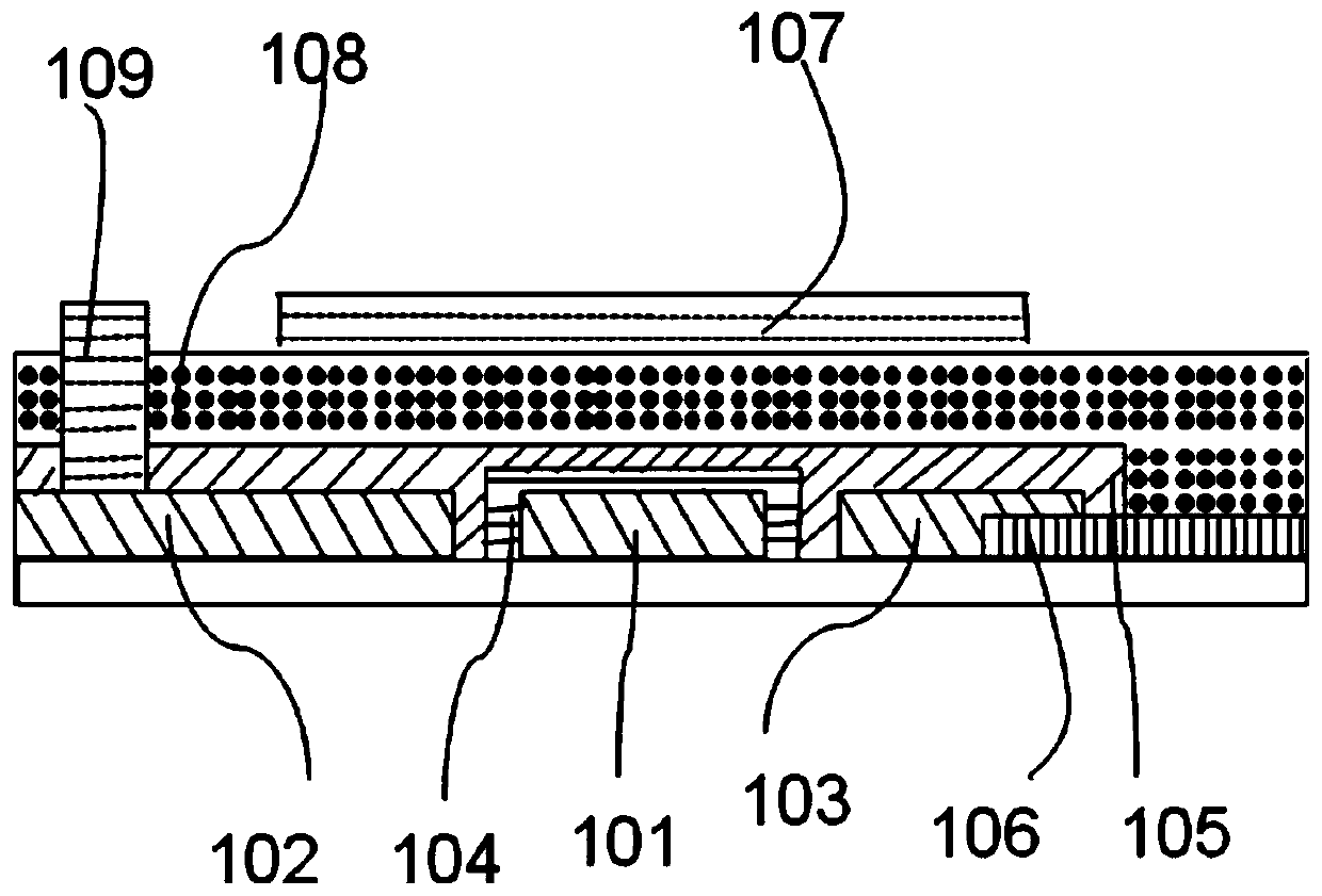
[0044] refer to figure 1 , which shows a schematic structural view of a thin film transistor according to Embodiment 1 of the present invention.

[0045] The thin film transistor includes: a first gate 101, a source 102 and a drain 103 located on the same layer on the substrate, a first gap is formed between the source 102 and the first gate 101, and the drain A second gap is formed between the electrode and the first grid.

[0046] A gate insulating layer 104 covering the first gate.

[0047] The semiconductor layer 105 covering the source 102 , the gate insulating layer 104 , the drain 103 and filling the first gap and the second gap.

[0048] In this structure, the substrate can be formed of a transparent glass material whose main component is silicon dioxide. The material forming the substrate is not limited to the transparent glass material, and can also be a transparent plastic material. The substrate is preferably a glass substrate.

[0049] In the same layer on the ...

Embodiment 2

[0069] The present invention also discloses a display panel, including the thin film transistor in the first embodiment.

[0070] The thin film transistor has all the advantages of the thin film transistor in the first embodiment above, which will not be repeated here.

Embodiment 3

[0072] The present invention also discloses a display device, including the display panel in the second embodiment.

[0073] It should be noted that the display device in this embodiment may be any product or component with a display function such as a mobile phone, a tablet computer, a television, a notebook computer, a digital photo frame, a navigator, and the like.

[0074] The display device has all the advantages of the display substrate in the second embodiment above, and will not be repeated here.


PUM


Abstract

The invention provides a thin film transistor and a manufacturing method thereof, a display panel and a display device. The thin film transistor comprises a first grid electrode, a source electrode and a drain electrode, which are arranged on a substrate and on the same layer, wherein a first gap is formed between the source electrode and the first grid electrode, and a second gap is formed between the drain electrode and the first grid electrode; a grid insulation layer covered on the first grid electrode; and a semiconductor layer covered on the source electrode, the grid insulation layer and the drain electrode and filling the first gap and the second gap. Therefore, the technological process of the bigrid thin film transistor is simplified, and product yield rate is improved.

Description

technical field [0001] The invention relates to the field of display technology, in particular to a thin film transistor and a manufacturing method thereof, a display panel, and a display device. Background technique [0002] TFT-LCD (Thin Film Transistor-Liquid Crystal Display) is currently the mainstream display product. In recent years, major panel manufacturers have been continuously expanding their production scale, and the market demand is increasing to improve production efficiency and produce high-quality liquid crystal display products. It is the key to occupying the market. [0003] In the prior art, the manufacture of thin film transistors requires a separate patterning process for the gate, and then a separate patterning process for the source and drain, and a gate insulating layer. During the above process , the gate, source and drain need to be processed separately, the manufacturing process of thin film transistors is relatively complicated, and the gap betwe...

Claims


Application Information

Patent Timeline
Patent Type & Authority Patents(China)
IPC IPC(8): H01L29/786H01L29/417H01L29/423H01L21/336H01L21/28
CPCH01L21/28H01L21/28008H01L29/41733H01L29/41775H01L29/42356H01L29/42384H01L29/66484H01L29/66742H01L29/78645
Inventor 周宏儒赵永亮毕鑫
Owner BOE TECH GRP CO LTD
Why Eureka
Try Eureka