Organic light-emitting device, manufacturing method thereof, display panel and display device

A technology for organic light-emitting devices and display panels, applied in semiconductor/solid-state device manufacturing, semiconductor devices, electric solid-state devices, etc., can solve the problem of increasing current density in non-dark spot areas, accelerating the deterioration of non-dark spot areas, and reducing the life of OLED devices and other problems, to achieve the effect of improving adhesion, increasing contact area, and avoiding black spots

Active Publication Date: 2017-09-01
WUHAN TIANMA MICRO ELECTRONICS CO LTD
View PDF9 Cites 4 Cited by
  • Summary
  • Abstract
  • Description
  • Claims
  • Application Information

AI Technical Summary

Problems solved by technology

In addition, the existence of dark spots will increase the current density in the non-black spot area, thereby accelerating the deterioration of the non-black spot area and reducing the life of the OLED device.

Method used


Image

  • Organic light-emitting device, manufacturing method thereof, display panel and display device
  • Organic light-emitting device, manufacturing method thereof, display panel and display device
  • Organic light-emitting device, manufacturing method thereof, display panel and display device

Examples


Embodiment Construction

[0037] The application will be further described in detail below in conjunction with the accompanying drawings and embodiments. It should be understood that the specific embodiments described here are only used to explain related inventions, rather than to limit the invention. It should also be noted that, for ease of description, only parts related to the invention are shown in the drawings.

[0038] It should be noted that, in the case of no conflict, the embodiments in the present application and the features in the embodiments can be combined with each other. The present application will be described in detail below with reference to the accompanying drawings and embodiments.

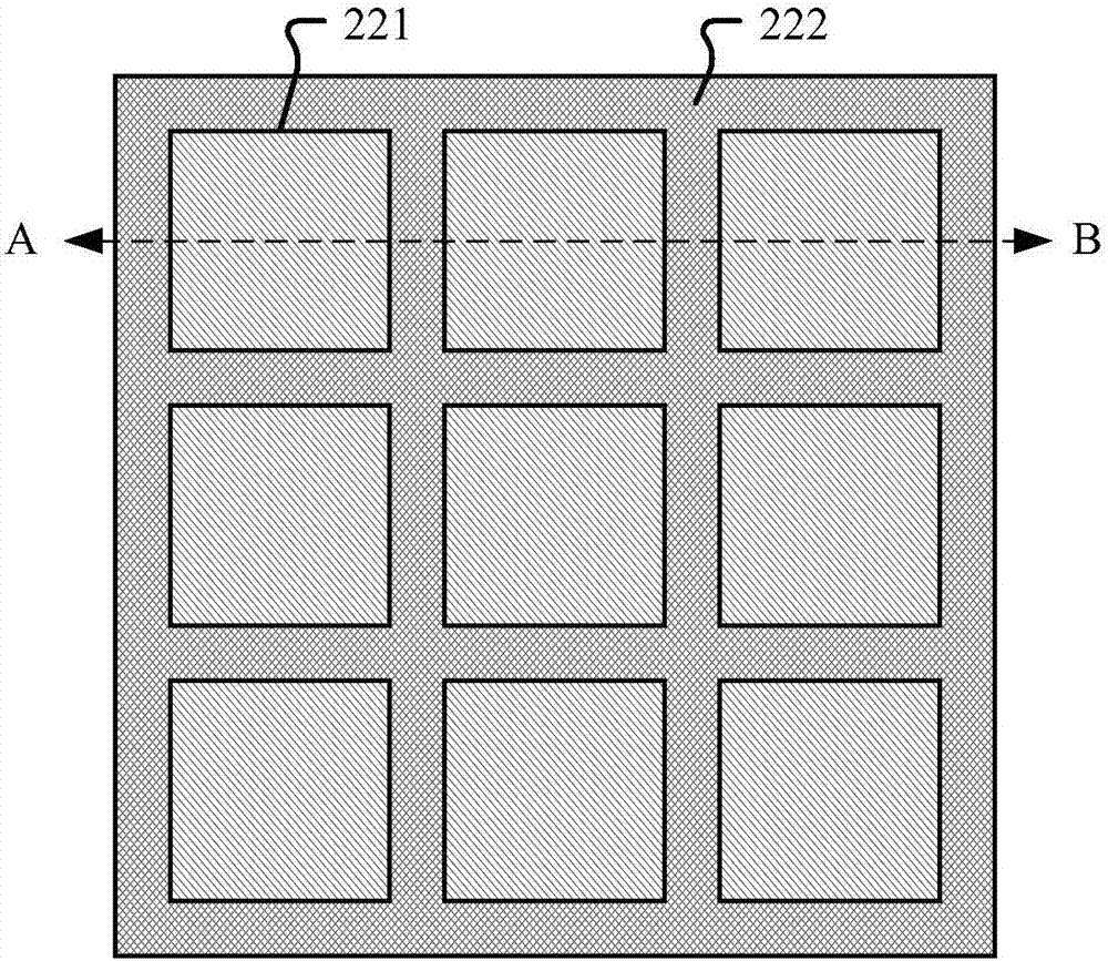
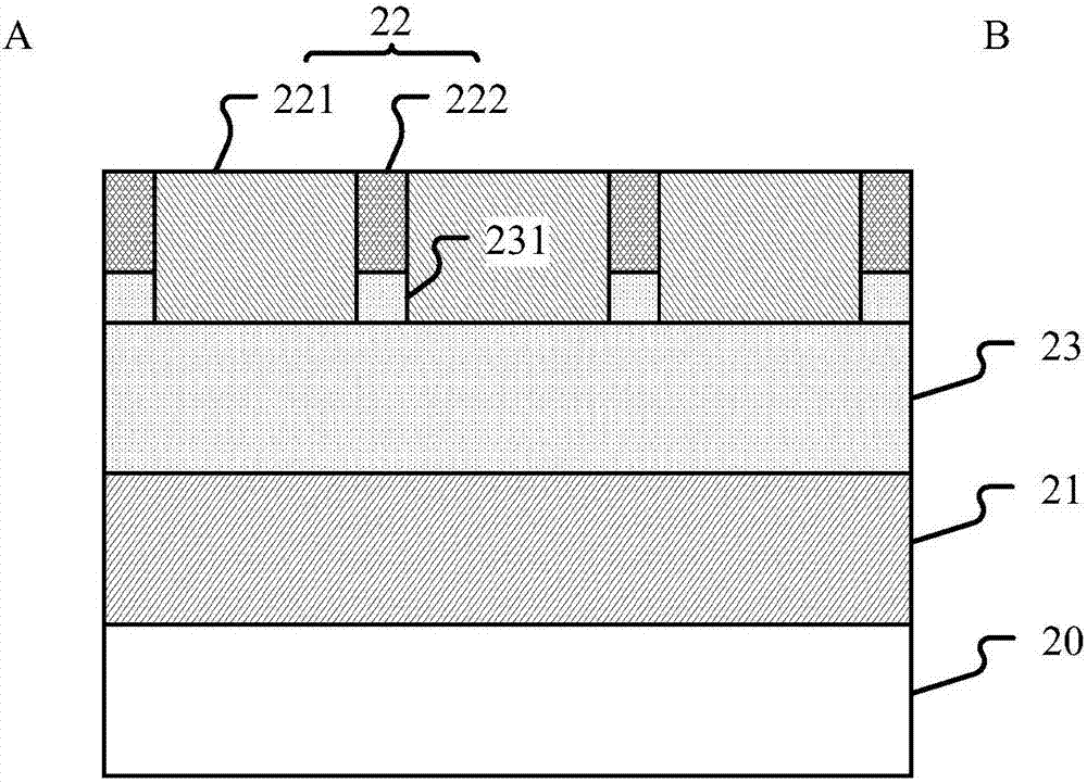
[0039] Figure 2A shows a top view of an organic light emitting device according to an embodiment of the present application, Figure 2B for along Figure 2A Cross-sectional view of line AB in.

[0040] Such as Figure 2A and Figure 2B As shown, the organic light emitting device may include ...


PUM


Abstract

The present application discloses an organic light-emitting device, a manufacturing method thereof, a display panel and a display device. The organic light-emitting device comprises a first electrode and a second electrode arranged on a substrate, and an organic light-emitting function layer positioned between the first and second electrodes. The second electrode comprises a plurality of second electrode blocks and second connection electrodes used for electrically connecting the second electrode blocks with one another. The organic light-emitting function layer comprises first organic material blocks configured to protrude towards the second connection electrodes. According to the technical scheme of the invention, organic material blocks configured to protrude towards the second connection electrodes are arranged on the organic light-emitting function layer, so that the contact area of the second electrodes with the organic light-emitting function layer is increased. The adhesive force between the second electrodes and the organic light-emitting function layer is improved, so that the generation of black spots is avoided.

Description

technical field [0001] The present application generally relates to the field of display technology, and in particular relates to an organic light emitting device, a manufacturing method thereof, a display panel and a display device. Background technique [0002] OLED (Organic Light Emitting Diode, Organic Light Emitting Diode), as an active light-emitting display device, has the advantages of high brightness, fast response, bendability, ultra-thin and no backlight, and has important applications in the field of display technology, especially becoming the most Display devices that have the potential to replace liquid crystal displays. [0003] A prior art OLED device may comprise an anode 11, a hole transport layer 13, a light emitting layer 15, an electron transport layer 14 and a cathode 12, such as figure 1 shown. When a driving voltage is applied to the cathode 12 and the anode 11, the holes from the hole transport layer 13 and the electrons from the electron transport...

Claims


Application Information

Patent Timeline
Patent Type & Authority Applications(China)
IPC IPC(8): H01L51/50H01L51/52H01L51/56
CPCH10K50/11H10K50/805H10K71/00
Inventor 张盎然王湘成王建云程爽
Owner WUHAN TIANMA MICRO ELECTRONICS CO LTD
Why Eureka
Try Eureka