

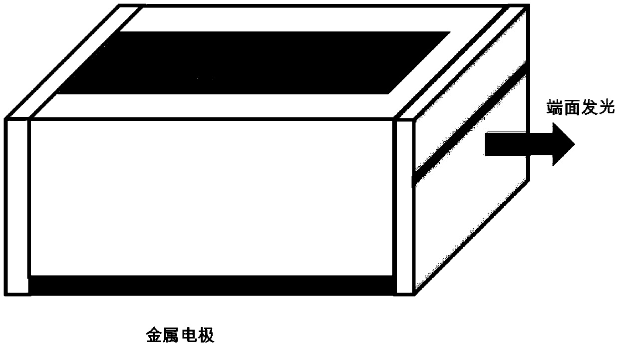
A small divergence angle laser and its manufacturing process
A preparation process, laser technology, applied in the direction of lasers, laser components, semiconductor lasers, etc., can solve the problems of packaging factory packaging efficiency and cost increase, unstable chip manufacturing process, affecting packaging production efficiency, etc., to reduce packaging costs and The effects of efficiency, large fault tolerance range, and increased modal stability
- Summary
- Abstract
- Description
- Claims
- Application Information
AI Technical Summary
Problems solved by technology
Method used
Image

Examples
Embodiment Construction
[0032] The present invention will be described in detail below in conjunction with the accompanying drawings and specific embodiments.
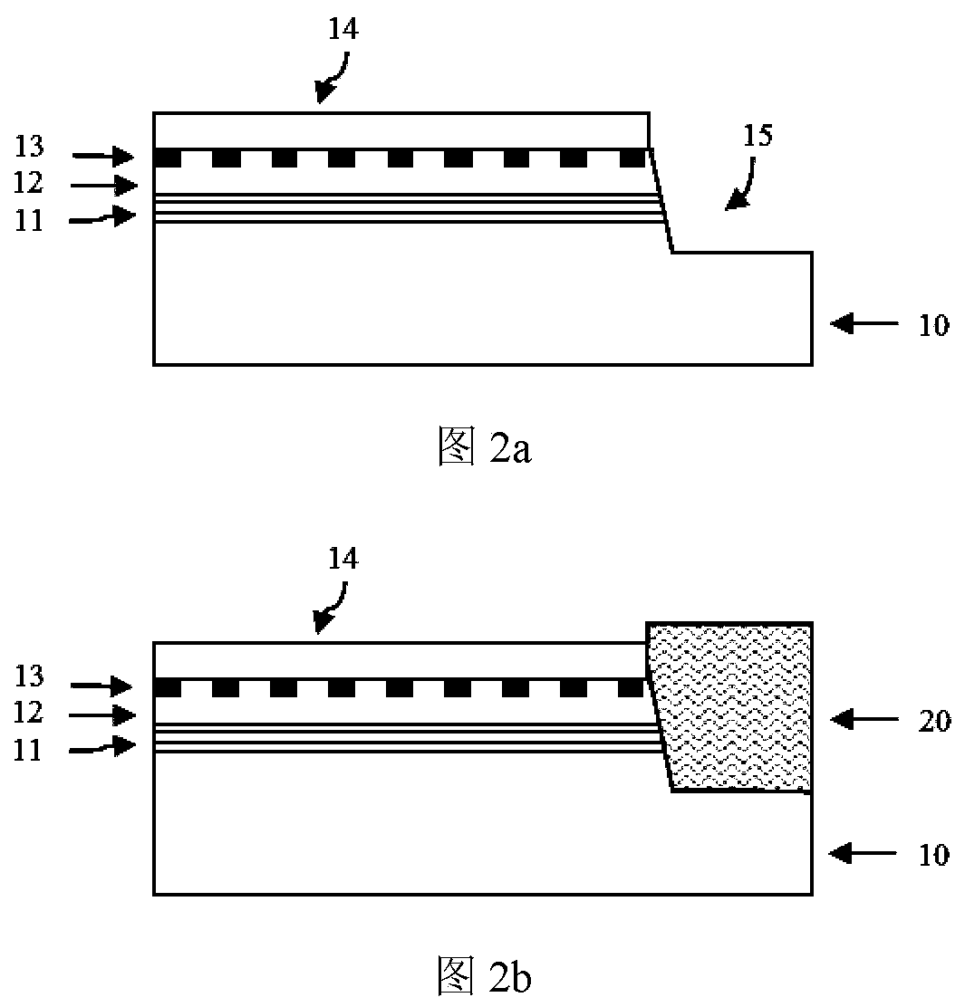
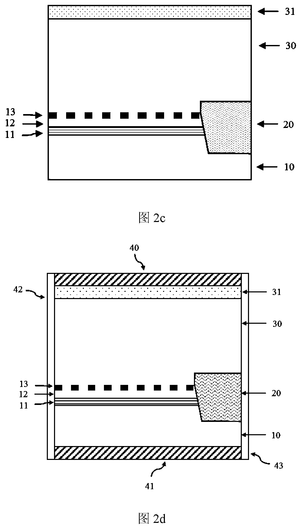
[0033] Such as figure 2 As shown in d, the small divergence angle laser of the present invention, a small divergence angle laser, includes a substrate 10 and an active region 11, a first cladding layer 12 and a diffraction grating layer 13 sequentially arranged on the substrate 10, the first cladding layer The layer 12 is made of InP material, the end of the first cladding layer 12 and the diffraction grating layer 13 are provided with an end surface etching region 15, the bottom of the end surface etching region 15 is located in the substrate 10, and a divergence angle improving layer 20 is grown in the end surface etching region 15 , the divergence angle improving layer 20 is an insulating InP material; the diffraction grating layer 13 and the divergence angle improving layer 20 are covered with a second cladding layer 30, a contact layer ...
PUM
 Abstract
Description
Claims
Application Information