Light emitting diode applied to parallel light illumination

A technology of light-emitting diodes and parallel light, which is applied in the direction of electrical components, circuits, semiconductor devices, etc., can solve the problems of small divergence angle, inability to obtain, and low radiation output, so as to reduce light radiation, optimize lighting design, and reduce light output area Effect

Active Publication Date: 2017-09-15
广东新克尔光电科技有限公司
View PDF3 Cites 2 Cited by
  • Summary
  • Abstract
  • Description
  • Claims
  • Application Information

AI Technical Summary

Problems solved by technology

[0016] The purpose of the present invention is to provide a light-emitting diode suitable for parallel light illumination, aiming

Method used


Image

  • Light emitting diode applied to parallel light illumination
  • Light emitting diode applied to parallel light illumination
  • Light emitting diode applied to parallel light illumination

Examples


Embodiment 1

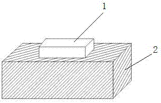
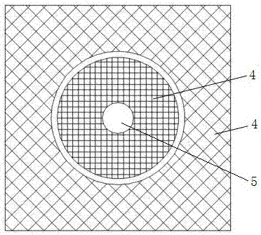
[0052] When both electrodes of the light emitting diode chip are located on the upper surface of the light emitting diode chip, such as Figure 5 As shown, the cover layer 4 is formed by two electrodes, and the two electrodes are designed to jointly cover the upper surface of the light-emitting diode chip 1 and only form a circular light exit hole 5 in the center. The diameter of the circular light exit hole 5 is preferably 0.1-0.5 mm. The area of ​​the two electrodes on the upper surface of the light-emitting diode chip 1 is much larger than the area of ​​the two electrodes of ordinary light-emitting diodes. Since the area of ​​the light-emitting area decreases, the total radiant flux decreases, but the radiation emission in the area of ​​the central circular light exit hole 5 increases. It is beneficial to reduce the divergence angle of parallel light. The corresponding light-emitting diode packaging structure is as follows: Figure 11 As shown, it includes a light emittin...

Embodiment 2

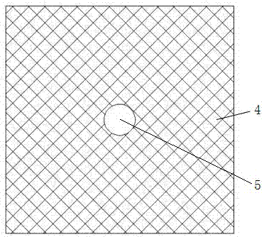
[0054] When the two electrodes of the light-emitting diode chip are respectively located on the upper surface and the lower surface of the light-emitting diode chip, such as Image 6 As shown, the cover layer 4 is formed by electrodes located on the upper surface of the LED chip 1, and the area of ​​the electrodes located on the upper surface of the LED chip 1 is increased so that the electrodes located on the upper surface of the LED chip 1 cover the upper surface of the LED chip 1 And only a circular light exit hole 5 is formed in the center, and the diameter of the circular light exit hole 5 is preferably 0.1-0.5 mm. Since the area of ​​the luminous area is reduced, the total radiant flux is reduced, but the radiation output degree in the area of ​​the central circular light exit hole 5 is increased, which is beneficial to reduce the divergence angle of the parallel light. The corresponding light-emitting diode packaging structure is as follows: Figure 11 As shown, it inc...

Embodiment 3

[0056] When the light-emitting diode adopts a flip-chip package structure and both electrodes are located on the lower surface of the light-emitting diode chip in contact with the heat sink, the substrate of the light-emitting diode chip 1 is located on the top of the light-emitting diode chip 1, such as Figure 7 As shown, the substrate 7 on the top of the LED chip 1 is thinned, so that the thickness of the remaining substrate 7 is 0-80 microns, or as Figure 8 As shown, the substrate 7 of the light-emitting diode chip 1 is completely peeled off, and the light-emitting area of ​​the four sides of the light-emitting diode chip 1 is reduced by thinning or peeling off the substrate, reducing the light radiation on the side, and, as Figure 9 As shown, the upper surface of the light-emitting diode chip 1 after thinning or peeling off the substrate is covered with a cover layer 4 that suppresses light radiation, and the cover layer 4 is a metal film plated on the upper surface of t...


PUM

PropertyMeasurementUnit
Thicknessaaaaaaaaaa

Abstract

The invention provides a light emitting diode applied to parallel light illumination. The light emitting diode comprises a light emitting diode chip, a heat sink and an optical packaging body. The lower surface of the light emitting diode chip contacts the heat sink, and the upper surface and four side surfaces are light emitting surfaces. The light emitting diode chip is coated by the optical packaging. Partial areas of the light emitting surfaces are covered by covering layers for inhibiting optical radiation. According to the light emitting diode, the partial areas of the light emitting surfaces of the light emitting diode chip are covered by the covering layers for inhibiting optical radiation, so the total radiation flux of the light emitting diode is inhibited and the unprocessed light emitting surface areas can obtain great radiant exitance. According to the light source, a divergence angle of parallel light is reduced, and the illumination design of the parallel light is optimized.

Description

technical field [0001] The invention relates to a light emitting diode (LED), in particular to a light emitting diode applied to parallel light illumination. Background technique [0002] The manufacturing of microelectronics and micro-electromechanical systems needs to be applied to the exposure machine. The optical system in the exposure machine converts the light emitted by the light source into ideal parallel light, and then transfers the size of the pattern on the mask to the mask under the parallel light. On the film, and then through etching, the pattern on the film is transferred to the substrate. In the whole manufacturing process, the divergence angle of the parallel light determines the accuracy of pattern transfer from the film to the substrate, the smaller the divergence angle, the higher the transfer accuracy. [0003] Traditional collimated light sources often use larger metal or metal halide gas discharge lamps, which have impure spectral lines, short lifesp...

Claims


Application Information

Patent Timeline
IPC IPC(8): H01L33/20H01L33/44H01L33/58
CPCH01L33/20H01L33/44H01L33/58
Inventor 王文峰刘一霖赵江熊晖张军
Owner 广东新克尔光电科技有限公司
Why Eureka
Try Eureka