Ink formula, photoelectric device and preparation method for functional layer of photoelectric device

A technology of optoelectronic devices and functional layers, which is applied in the fields of electrical solid devices, chemical instruments and methods, semiconductor/solid device manufacturing, etc., and can solve problems such as uneven film layers

Active Publication Date: 2017-09-19
NANJING TECH CORP LTD
View PDF8 Cites 14 Cited by
  • Summary
  • Abstract
  • Description
  • Claims
  • Application Information

AI Technical Summary

Problems solved by technology

[0006] The main purpose of the present invention is to provide an ink formula, a photoelectric device and a method for preparing the functional la

Method used


Image

  • Ink formula, photoelectric device and preparation method for functional layer of photoelectric device
  • Ink formula, photoelectric device and preparation method for functional layer of photoelectric device

Examples


preparation example Construction

[0048] In another typical embodiment of the present application, a method for preparing a functional layer of a photoelectric device is provided, the preparation method comprising: setting A component as the first preliminary layer; setting B component in the first preliminary layer Form the second preparatory layer on the preform to obtain a preform; dry the preform to obtain the functional layer of the photoelectric device; wherein, the A component and the B group are respectively the A component and the B component in any of the above-mentioned ink formulations . The optoelectronic device can be an electroluminescent device or a solar cell or a photovoltaic cell. The aforementioned drying treatment may be any drying treatment, such as vacuum drying, infrared drying or oven drying, etc., preferably in a manner that does not affect the performance of the functional layer during drying. The timing of the aforementioned drying treatment may be after the preparatory layer of on...

Embodiment 1-8

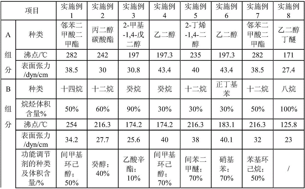
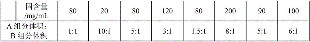
[0060] The functional materials in Examples 1-8 are all luminescent nanocrystals (red quantum dots, CdSe / ZnS with oleylamine ligands), and the types and amounts of components in the ink formulations of each example are as follows.

[0061] Table 1:

[0062]

[0063]

[0064] The ink formula inkjet printing (printer model is DMP2831) of above-mentioned each embodiment is on transparent glass substrate, uses Filmetrics F40 model machine to test film thickness, evenly gets nine positions to test, then calculates thickness uniformity=(Max-Min ) / (2Ave), and Ave=(d1+d2+d3+...+d8+d9) / 9, where Max refers to the value with the largest thickness among the 9 data, Min refers to the value with the smallest thickness, and Ave refers to each The average thickness of the point, d1, d2...d9 represent the thickness value of each point. The smaller the value of thickness uniformity, the more uniform the film thickness. The test results of the thickness uniformity of each embodiment are ...


PUM


Abstract

The invention provides an ink formula, a photoelectric device and a preparation method for the functional layer of the photoelectric device. The ink comprises a component A and a component B, wherein the component A comprises first liquid; the component B comprises second liquid and functional materials dispersed in the second liquid; the boiling point of the first liquid is higher than the boiling point of the second liquid by at least ten DEG C; the first liquid and the second liquid do not mutually dissolve; the solubility of the functional materials in the second liquid is higher than or equal to 1g, and the solubility of the functional materials in the first liquid is less than or equal to 0.05g; the density of the first liquid is greater than the density of the second liquid; the range of a ratio of the surface tension of the first liquid to the surface tension of the second liquid is 0.8-1.2; the second liquid is volatilized earlier than the first liquid; along with the volatilization of the second liquid, two parallel interfaces are formed between the component B and external atmosphere as well as the component A; along with the volatilization of the first liquid, solids which are evenly dispersed on the interface form an even film layer on a matrix so as to solve the problem of unevenness in film formation.

Description

technical field [0001] The invention relates to the field of luminescent material solutions, in particular to an ink formulation, a photoelectric device and a method for preparing a functional layer of the photoelectric device. Background technique [0002] The coffee ring phenomenon or the phenomenon of ink accumulation in the middle of the solution method printing to prepare the light-emitting device leads to uneven film layer, which makes the light emission uneven. [0003] In the prior art, there is a method for preparing an organic light-emitting material solution that uses convection to improve the uniformity of inkjet printing films, which includes two solvents, the first solvent is chlorobenzene, and the second solvent is cumene. The boiling points of these two solvents are If the temperature is below 160°C and the viscosity is below 1cps, not only the quality of ink output from the nozzle will be affected, but also the drying speed of the solvent will be faster, whi...

Claims


Application Information

Patent Timeline
IPC IPC(8): C09D11/54H01L51/54H01L51/56
CPCC09D11/54H10K71/15H10K71/135H10K71/00C09D11/50C09D11/52C09D11/322C09D11/38C09D11/40C09K11/025B82Y20/00B82Y40/00H10K50/11H10K50/115H10K2101/10
Inventor 郭海涛彭军军甄常刮
Owner NANJING TECH CORP LTD
Why Eureka
Try Eureka