Array base plate, display module, electronic equipment, fingerprint recognition method and fingerprint recognition device

An array substrate and fingerprint identification technology, applied in the electronic field, can solve the problems of limited fingerprint chip size, inconvenient use for users, cumbersome process, etc., and achieve the effects of flexible design, reduced difficulty, and convenient use

Inactive Publication Date: 2017-09-22
SHANGHAI YUDE TECH CO LTD
View PDF6 Cites 12 Cited by
  • Summary
  • Abstract
  • Description
  • Claims
  • Application Information

AI Technical Summary

Problems solved by technology

[0003] The inventors of the present invention found in the process of realizing the present invention that: since the current fingerprint identification modules in mobile phones are mostly based on the principle of capacitance, and by packaging the fingerprint sensing chip made by the wafer process in an LGA (Land Grid Array) ) Packaging technology After being packaged into a module, it is then integrated into mobile phone products. Therefore, limited by the size of the fingerprint chip, the area where the fingerprint recognition function can be realized is currently very small, and it is very inconvenient for users to use.
Moreover, the fingerprint identification module needs to be packaged separately and then assembled into electronic equipment, which is a cumbersome process.

Method used


Image

  • Array base plate, display module, electronic equipment, fingerprint recognition method and fingerprint recognition device
  • Array base plate, display module, electronic equipment, fingerprint recognition method and fingerprint recognition device
  • Array base plate, display module, electronic equipment, fingerprint recognition method and fingerprint recognition device

Examples


Embodiment Construction

[0029] In order to make the object, technical solution and advantages of the present invention clearer, various embodiments of the present invention will be described in detail below in conjunction with the accompanying drawings. However, those of ordinary skill in the art can understand that, in each implementation manner of the present invention, many technical details are provided for readers to better understand the present application. However, even without these technical details and various changes and modifications based on the following implementation modes, the technical solution claimed in this application can also be realized.

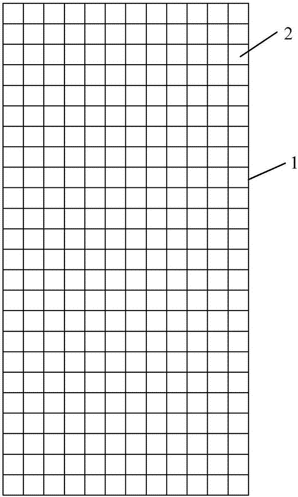
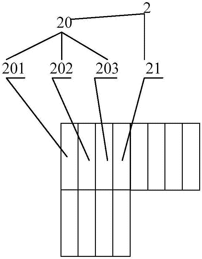
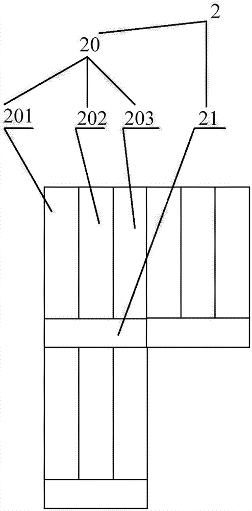
[0030] The first embodiment of the present invention relates to an array substrate, which is applied in a display module. Wherein, the display module can be an AMOLED (Active Matrix / Organic Light Emitting Diode, active matrix organic light emitting diode) display module, an LCD (Liquid Crystal Display, liquid crystal display) display module...


PUM


Abstract

The invention relates to an electronic technology, and discloses an array base plate, a display module, electronic equipment, a fingerprint recognition method and a fingerprint recognition device. The array base plate comprises a base plate body and first basic points, wherein the first basic points are arranged on the base plate body in a matrix manner; the first basic points comprise display pixels and fingerprint pixels which are arranged together; and the base plate body also comprises signal lines with the display pixels and the fingerprint pixels. The embodiment of the invention also provides a display module comprising the array base plate, electronic equipment comprising the display module and a fingerprint recognition method applied to the electronic equipment. Through the embodiment, the fingerprint pixels and the display pixels are integrated, so that the fingerprint collection can be simultaneously realized in a display region of the display device; therefore the fingerprint recognition region can be conveniently increased; the use by a user is convenient; and the fingerprint recognition module does not need to be singly integrated into the electronic equipment in the later period, so that the structural design difficulty of the electronic equipment can be reduced.

Description

technical field [0001] The invention relates to the field of electronic technology, in particular to an array substrate, a display module, electronic equipment, and a fingerprint identification method and device. Background technique [0002] Nowadays, fingerprint recognition technology is widely used in electronic devices (such as smart phones and tablet computers). Most of the existing fingerprint identification schemes are based on the capacitive principle (it uses semiconductor capacitor array sensing to measure the capacitance change of each pixel point, each pixel point is a capacitive electrode, when the finger is pressed on the fingerprint module identification area, according to the fingerprint The difference in the capacitance value of the valley and the fingerprint ridge realizes the fingerprint recognition function). At present, the fingerprint module of the mobile phone is generally arranged at the position of the front button, and such a fingerprint module gen...

Claims


Application Information

Patent Timeline
Patent Type & Authority Applications(China)
IPC IPC(8): G06F3/044G06K9/00
CPCG06F3/044G06V40/1306
Inventor 杨朝蓉欧阳慧军黄青青
Owner SHANGHAI YUDE TECH CO LTD
Why Eureka
Try Eureka