

Flexible electronic device and manufacturing method therefor
A flexible electronic device and a flexible technology, applied in the direction of electric solid devices, electrical components, semiconductor devices, etc., can solve the problems of electrical performance and anti-kneading performance of electronic devices, and achieve the effect of ensuring electrical performance and anti-kneading performance.
- Summary
- Abstract
- Description
- Claims
- Application Information
AI Technical Summary
Problems solved by technology
Method used
Image

Examples
Embodiment 1
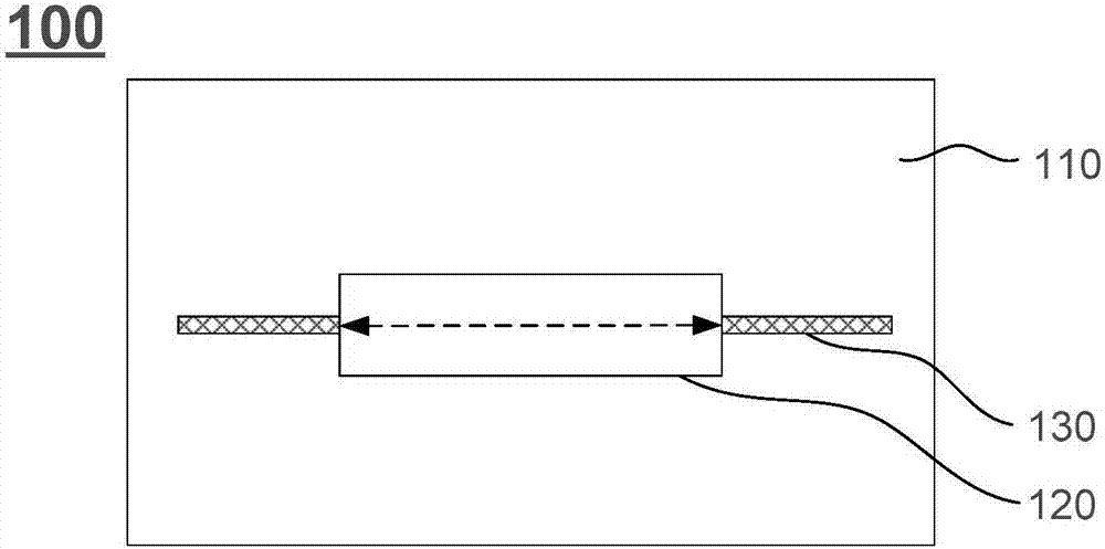
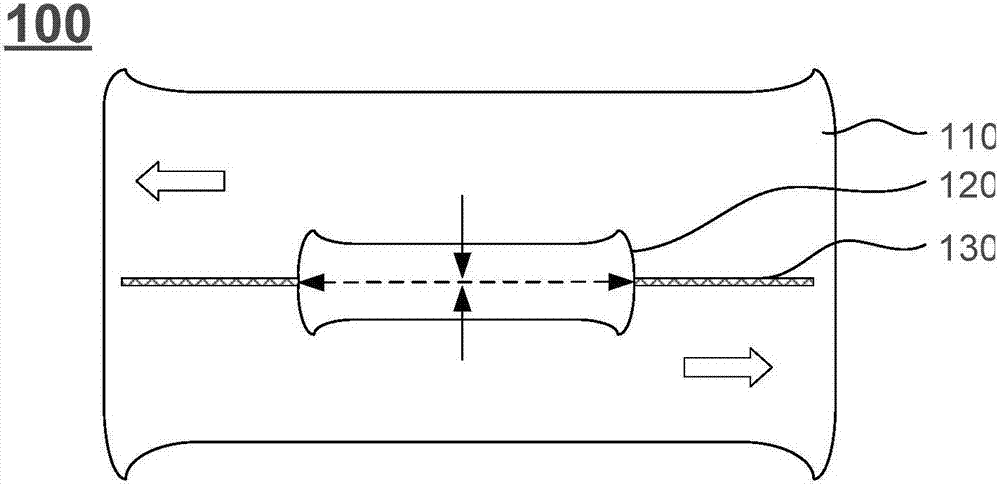
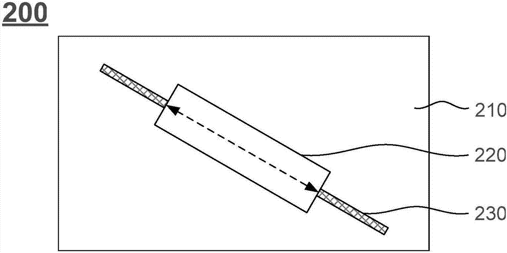
[0034] Please refer to image 3 , which is a schematic structural diagram of a flexible electronic device according to an embodiment of the present invention. Such as image 3 As shown, the flexible electronic device 200 includes: a flexible substrate 210 and a device layer formed on the flexible substrate 210; the device layer includes an interconnected semiconductor structure 220 and a first wire structure 230, and the first The extension direction of the wire structure 230 is consistent with the channel direction of the semiconductor structure 220 ; the extension direction of the first wire structure 230 and the stretching direction of the flexible substrate 210 form an angle less than 90°. The semiconductor structure in the embodiment of the present invention is a thin film transistor structure, specifically including a gate, a drain (not shown in the figure), and a channel.
[0035] Specifically, in the flexible electronic device 200, the device layer includes an interc...
Embodiment 2
[0049] Please refer to Figure 5 , which is a schematic structural diagram of a flexible electronic device according to Embodiment 2 of the present invention. Such as Figure 5 As shown, the flexible electronic device 300 includes: a flexible substrate 310 and a device layer 330 formed on the flexible substrate 310; the device layer 330 includes interconnected semiconductor structures (not shown in the figure) and a first A wire structure (not shown in the figure), the extension direction of the first wire structure is consistent with the channel direction of the semiconductor structure; the extension direction of the first wire structure is formed with the stretching direction of the flexible substrate 310 Angles less than 90°.
[0050] Specifically, in the flexible electronic device 300, the device layer 330 includes a plurality of pixel units 30 and a first wire structure, the plurality of pixel units 30 are arranged in an array, and each pixel unit 30 has a switch functi...
PUM
| Property | Measurement | Unit |
|---|---|---|
| Angle | aaaaa | aaaaa |
Abstract
Description
Claims
Application Information