

A method for obtaining nbti degradation model based on non-uniform distribution of interface traps
A non-uniform distribution, interface trap technology, applied in design optimization/simulation, instrumentation, informatics, etc., can solve the problem of accurate calculation of interface trap distribution in the channel edge region, and achieve wide applicability, accurate device reliability, and simulation. effect with fewer parameters
- Summary
- Abstract
- Description
- Claims
- Application Information
AI Technical Summary
Problems solved by technology
Method used
Image

Examples
Embodiment Construction
[0042] The present invention will be further described in detail in conjunction with the following specific embodiments and accompanying drawings. The process, conditions, experimental methods, etc. for implementing the present invention, except for the content specifically mentioned below, are common knowledge and common knowledge in this field, and the present invention has no special limitation content.
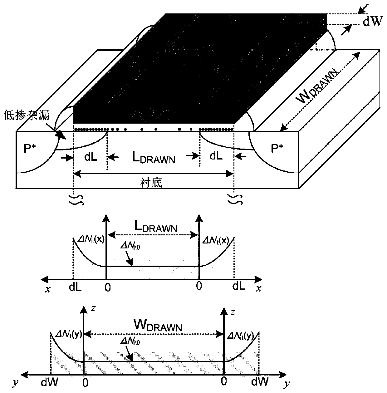
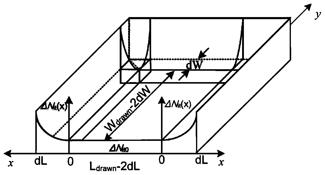
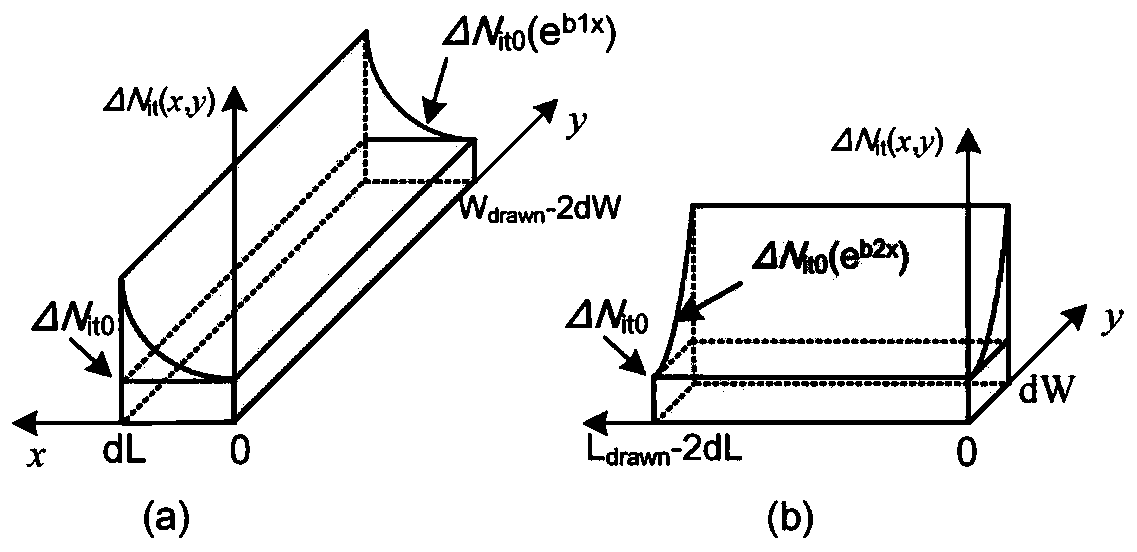
[0043] The NBTI degradation model provided by the present invention is based on the non-uniform distribution of interface traps, taking into account the influence of device geometry channel length and width, and accurately calculates the distribution frame and total density of interface traps. The modeling process of the present invention includes the following steps:
[0044] Step 1: Divide the interface trap ΔN in different regions of the MOS device IT distributed
[0045] according to figure 1 The schematic diagram of the distribution division of ΔNit is shown, and t...
PUM
 Abstract
Description
Claims
Application Information