Level shifting circuit

A technology for transferring circuits and levels, applied in logic circuits, eliminating voltage/current interference, logic circuit connection/interface layout, etc., can solve problems such as increased power consumption, large peak current, and device reliability, and achieve guaranteed drive capability, increase flip speed, and reduce power consumption

Active Publication Date: 2017-09-29
BOE TECH GRP CO LTD
View PDF5 Cites 5 Cited by
  • Summary
  • Abstract
  • Description
  • Claims
  • Application Information

AI Technical Summary

Problems solved by technology

[0004] However, the level conversion circuit with this structure has a limited driving capability and cannot drive a larger load. Therefore, in the prior art, the figure 1 Based on the method of connecting high-voltage inverters in series, we get figure 2 The level shifting circuit, thereby improving the driving ability of the level shifting circuit
Wherein, the high-voltage inverter includes a fifth transistor M5 (which is a PMOS transistor) and a sixth transistor M6 (which is an NMOS transistor). During the inversion process of the high-voltage inverter (that is, the gate of the fifth transistor M5 receives The signal is in a certain stage during the high-level and low-level conversion process), the fifth transistor M5 and the sixth transistor M6 will be in a weak open state at the same time, the first high-level signal terminal V1 and the low-level signal terminal VSS conduction between them, resulting in a large peak current, which will not only increase power consumption, but also affect the reliability of the device

Method used


Image

  • Level shifting circuit
  • Level shifting circuit
  • Level shifting circuit

Examples


Embodiment Construction

[0043] Specific embodiments of the present invention will be described in detail below in conjunction with the accompanying drawings. It should be understood that the specific embodiments described here are only used to illustrate and explain the present invention, and are not intended to limit the present invention.

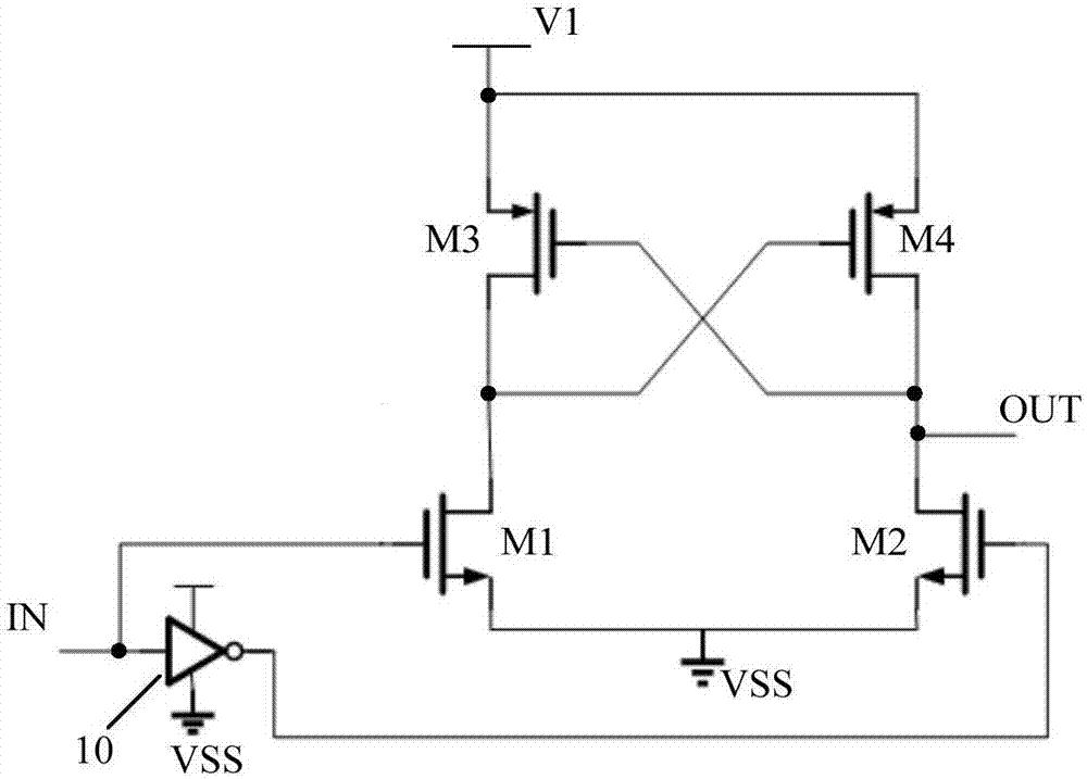
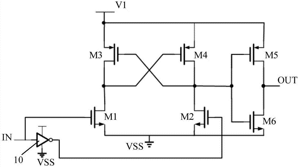
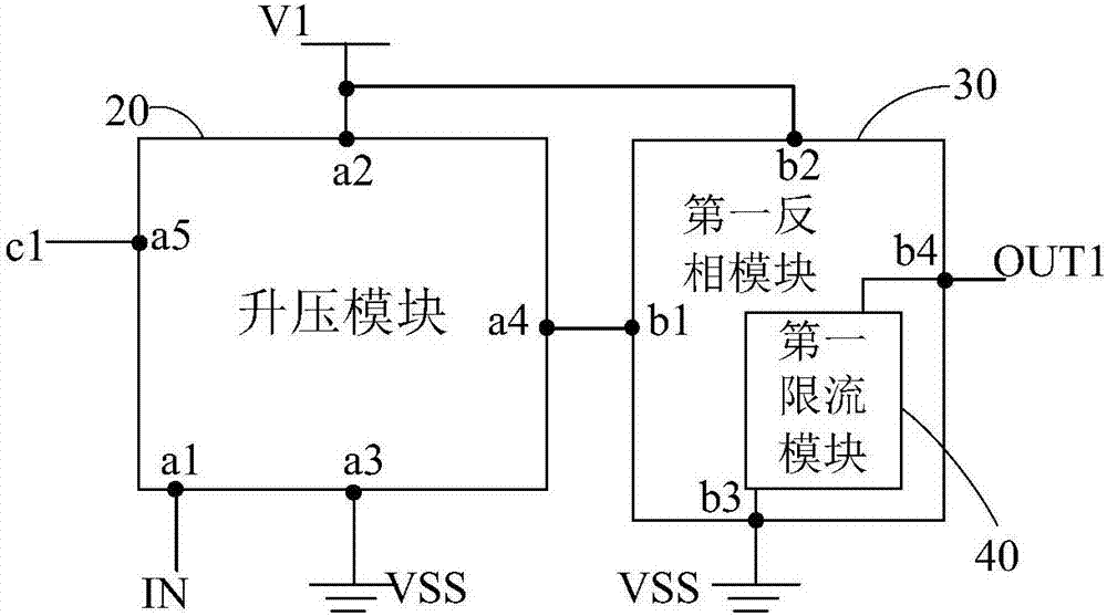
[0044] As an aspect of the present invention, a level shift circuit is provided, such as image 3 As shown, the level shift circuit includes a boost module 20 and a first inverting module 30 .

[0045] The first terminal a1 of the boost module 20 is connected to the input terminal IN of the level shift circuit, the second terminal a2 of the boost module 20 is connected to the first high-level signal terminal V1, and the third terminal a3 of the boost module 20 is connected to the input terminal IN of the level shift circuit. The low-level signal terminal VSS is connected, and the fourth terminal a4 of the boost module 20 is connected to the first terminal b1 of...


PUM


Abstract

The invention provides a level shifting circuit. The level shifting circuit comprises a booster module and a first phase reversal module; the first end of the booster module is connected with the input end of the level shifting circuit, the second end of the booster module is connected with a first high level signal end, the third end of the booster module is connected with a low level signal end, and the fourth end of the booster module is connected with the first end of the first phase reversal module; the second end of the first phase reversal module is connected with the first high level signal end, the third end of the first phase reversal module is connected with the low level signal end, and the fourth end of the first phase reversal module is connected with the first output end of the level shifting circuit; the first phase reversal module is used for communicating the third end and the fourth end of the first phase reversal module when the first end receives a high level signal; the first phase reversal module is used for communicating the second end and the fourth end of the first phase reversal module when the first end receives a low level signal; and a first current limiting module is arranged between the second end and the fourth end or between the third end and the fourth end of the first phase reversal module, and the first current limiting module is used for limiting current passing through the current limiting module per se to enable the maximum current value to be not greater than a first preset value. The invention can reduce peak current while improving the driving capability.

Description

technical field [0001] The invention relates to the field of semiconductor integrated circuits, in particular to a level shift circuit. Background technique [0002] The level shift circuit converts the low-voltage control signal into a high-voltage control signal, and realizes the control of the low-voltage logic to the high-voltage power output stage. It has a wide range of applications in organic electroluminescence, FLASH storage, etc. As a key circuit connecting the control circuit and the output driver stage, the level shift circuit requires high driving capability to meet the driving requirements of the output stage on the one hand; on the other hand, it requires relatively low quiescent current to reduce power consumption. [0003] figure 1 It is a structural diagram of a traditional level shift circuit, including four transistors (first transistor M1 , second transistor M2 , third transistor M3 and fourth transistor M4 ) and a low-voltage inverter 10 . The first t...

Claims


Application Information

Patent Timeline
Patent Type & Authority Applications(China)
IPC IPC(8): H03K19/0185
CPCH03K19/018507H03K19/00361H03K19/018521
Inventor 王糖祥
Owner BOE TECH GRP CO LTD
Why Eureka
Try Eureka