Tristate phase inverter based on FinFET device

A technology of tri-state inverters and devices, applied to logic circuits with logic functions, etc., can solve problems such as increased leakage current, unimproved tri-state inverter area, and increased leakage power consumption

Inactive Publication Date: 2017-09-29
NINGBO UNIV
View PDF2 Cites 0 Cited by
  • Summary
  • Abstract
  • Description
  • Claims
  • Application Information

AI Technical Summary

Problems solved by technology

The circuit of the traditional three-state inverter (that is, the classic three-state inverter in the BSIMIMG process library) is as follows: figure 1 As shown, the tri-state inverter is composed of three NMOS transistors and three PMOS transistors. Due to the sharp increase of leakage current below the 45nm technology node, the leakage power consumption continues to increase, resulting in unbearable excessive power consumption; The area occupied by the three-state inverter connected to the bus has not been improved, especially after the emergence of a large number of portable devices such as mobile phones, PDAs and notebook computers, the requirements for small area and low power consumption are more urgent

Method used


Image

  • Tristate phase inverter based on FinFET device
  • Tristate phase inverter based on FinFET device
  • Tristate phase inverter based on FinFET device

Examples


Embodiment 1

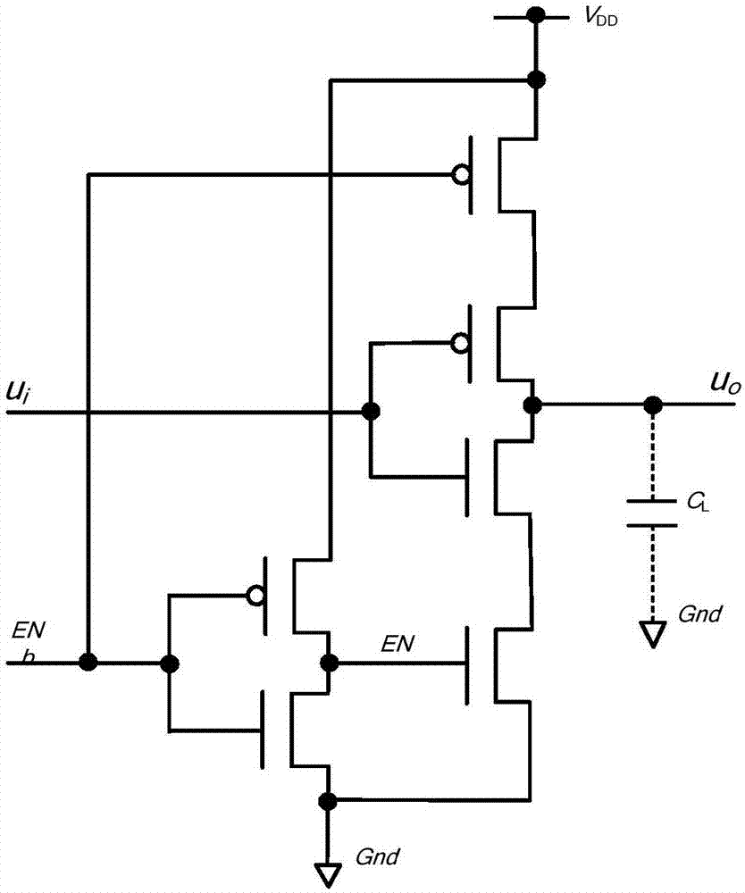
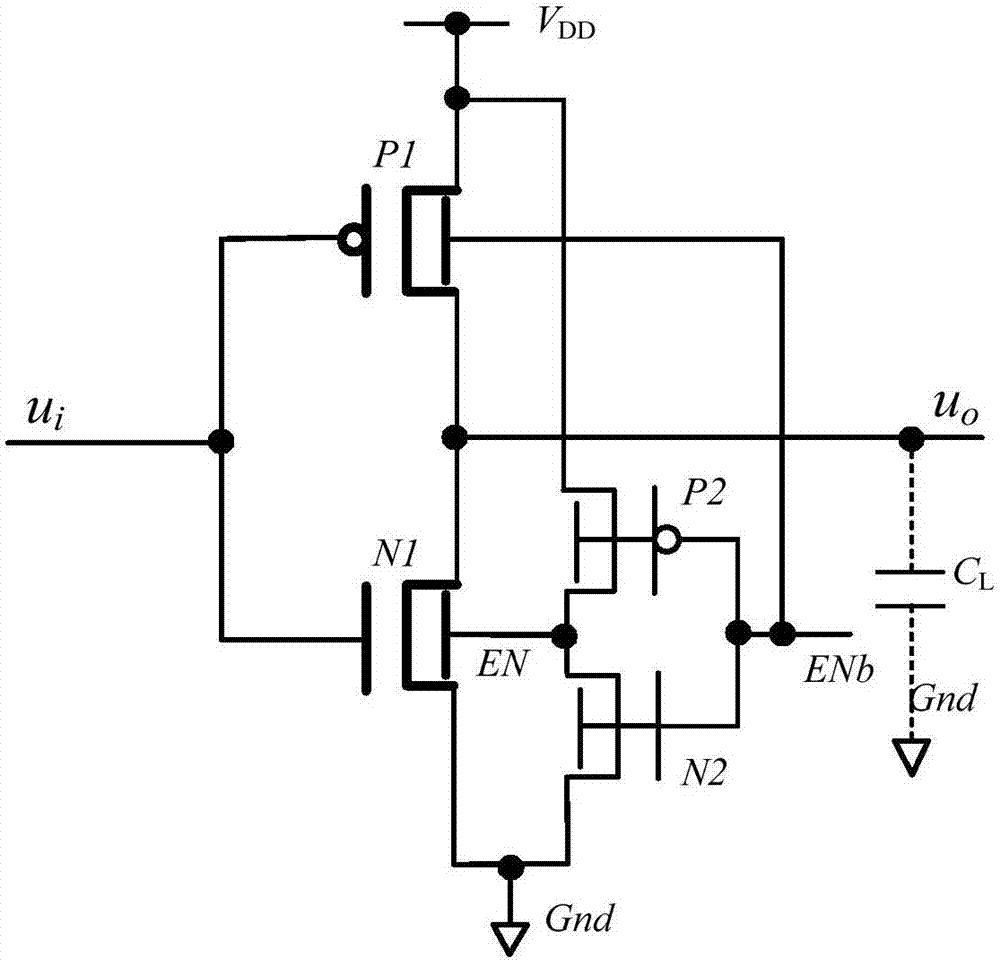
[0015] Embodiment one: if figure 2 As shown, a tri-state inverter based on FinFET devices includes a first N-type FinFET transistor N1, a second N-type FinFET transistor N2, a first P-type FinFET transistor P1, and a second P-type FinFET transistor P2. The P-type FinFET P1 is a high-threshold P-type FinFET, the first N-type FinFET N1 is a high-threshold N-type FinFET, the second P-type FinFET P2 is a low-threshold P-type FinFET, and the second N-type FinFET N2 It is a low-threshold N-type FinFET; the source of the first P-type FinFET P1 and the source of the second P-type FinFET P2 are connected to the power supply VDD, and the front gate of the first P-type FinFET P1 and the first N-type The front gate of the FinFET tube N1 is connected and its connection end is the input terminal of the tri-state inverter, the back gate of the first P-type FinFET tube P1, the front gate of the second P-type FinFET tube P2, and the second P-type FinFET tube P2 The back gate of the second N-...

Embodiment 2

[0016] Embodiment two: if figure 2 As shown, a tri-state inverter based on FinFET devices includes a first N-type FinFET transistor N1, a second N-type FinFET transistor N2, a first P-type FinFET transistor P1, and a second P-type FinFET transistor P2. The P-type FinFET P1 is a high-threshold P-type FinFET, the first N-type FinFET N1 is a high-threshold N-type FinFET, the second P-type FinFET P2 is a low-threshold P-type FinFET, and the second N-type FinFET N2 It is a low-threshold N-type FinFET; the source of the first P-type FinFET P1 and the source of the second P-type FinFET P2 are connected to the power supply VDD, and the front gate of the first P-type FinFET P1 and the first N-type The front gate of the FinFET tube N1 is connected and its connection end is the input terminal of the tri-state inverter, the back gate of the first P-type FinFET tube P1, the front gate of the second P-type FinFET tube P2, and the second P-type FinFET tube P2 The back gate of the second N-...

Embodiment 3

[0018] Embodiment three: as figure 2As shown, a tri-state inverter based on FinFET devices includes a first N-type FinFET transistor N1, a second N-type FinFET transistor N2, a first P-type FinFET transistor P1, and a second P-type FinFET transistor P2. The P-type FinFET P1 is a high-threshold P-type FinFET, the first N-type FinFET N1 is a high-threshold N-type FinFET, the second P-type FinFET P2 is a low-threshold P-type FinFET, and the second N-type FinFET N2 It is a low-threshold N-type FinFET; the source of the first P-type FinFET P1 and the source of the second P-type FinFET P2 are connected to the power supply VDD, and the front gate of the first P-type FinFET P1 and the first N-type The front gate of the FinFET tube N1 is connected and its connection end is the input terminal of the tri-state inverter, the back gate of the first P-type FinFET tube P1, the front gate of the second P-type FinFET tube P2, and the second P-type FinFET tube P2 The back gate of the second N...


PUM


Abstract

The invention discloses a tristate phase inverter based on a FinFET device. The tristate phase inverter comprises the first N-type FinFET tube, a second N-type FinFET tube, the first P-type FinFET tube and the second P-type FinFET tube, wherein the first P-type FinFET tube is the high-threshold P-type FinFET tube, the first N-type FinFET tube is the high-threshold N-type FinFET tube; the second P-type FinFET tube is the low-threshold P-type FinFET tube, and the second N-type FinFET tube is the low-threshold N-type FinFET tube; the advantage is that the functions of two P-type FinFET tubes of a phase-reversing tube and an enabling tube are realized through the first P-type FinFET tube, the first N-type FinFET tube further realizes the effect of integrating the joint control of the input end and the enabling end; the functions of two N-type FinFET tubes of the phase-revering tube and the enabling tube are realized through the first N-type FinFET tube, and the circuit area, the time delay, the power consumption, and the power delay product are greatly optimized.

Description

technical field [0001] The invention relates to a three-state inverter, in particular to a three-state inverter based on a FinFET device. Background technique [0002] As the process size enters the nanometer level, power consumption has become a problem that IC designers have to pay attention to. Many new products that process electronic information, including microprocessors, memories, and data buses in digital signal processors and portable electronic information devices, not only require input / output (I / O) for isolation, buffering, or a certain logic function. ) Terminal tri-state buffer / driver or tri-state logic gate circuit, and the tri-state gate circuit is required to have low power supply voltage level, fast, low power consumption and high integration performance. [0003] A three-state inverter is a widely used three-state gate circuit. The circuit of the traditional three-state inverter (that is, the classic three-state inverter in the BSIMIMG process library) i...

Claims


Application Information

Patent Timeline
Patent Type & Authority Applications(China)
IPC IPC(8): H03K19/20
CPCH03K19/20
Inventor 胡建平杨会山汪佳峰
Owner NINGBO UNIV
Why Eureka
Try Eureka