Quantum dot, ink and quantum dot light emitting display device

A technology for quantum dot light-emitting and display devices, which is applied in the fields of electric solid-state devices, semiconductor devices, semiconductor/solid-state device manufacturing, etc.

Active Publication Date: 2017-10-03
NANJING TECH CORP LTD
View PDF4 Cites 12 Cited by
  • Summary
  • Abstract
  • Description
  • Claims
  • Application Information

AI Technical Summary

Problems solved by technology

[0003] The main purpose of this application is to provide a quantum dot, ink and quantum dot light-emitting display device to solve the problem that the QLED device in the prior art cannot improve the luminous efficiency while maintaining the stability of the quantum dot

Method used


Image

  • Quantum dot, ink and quantum dot light emitting display device
  • Quantum dot, ink and quantum dot light emitting display device

Examples


Embodiment 1

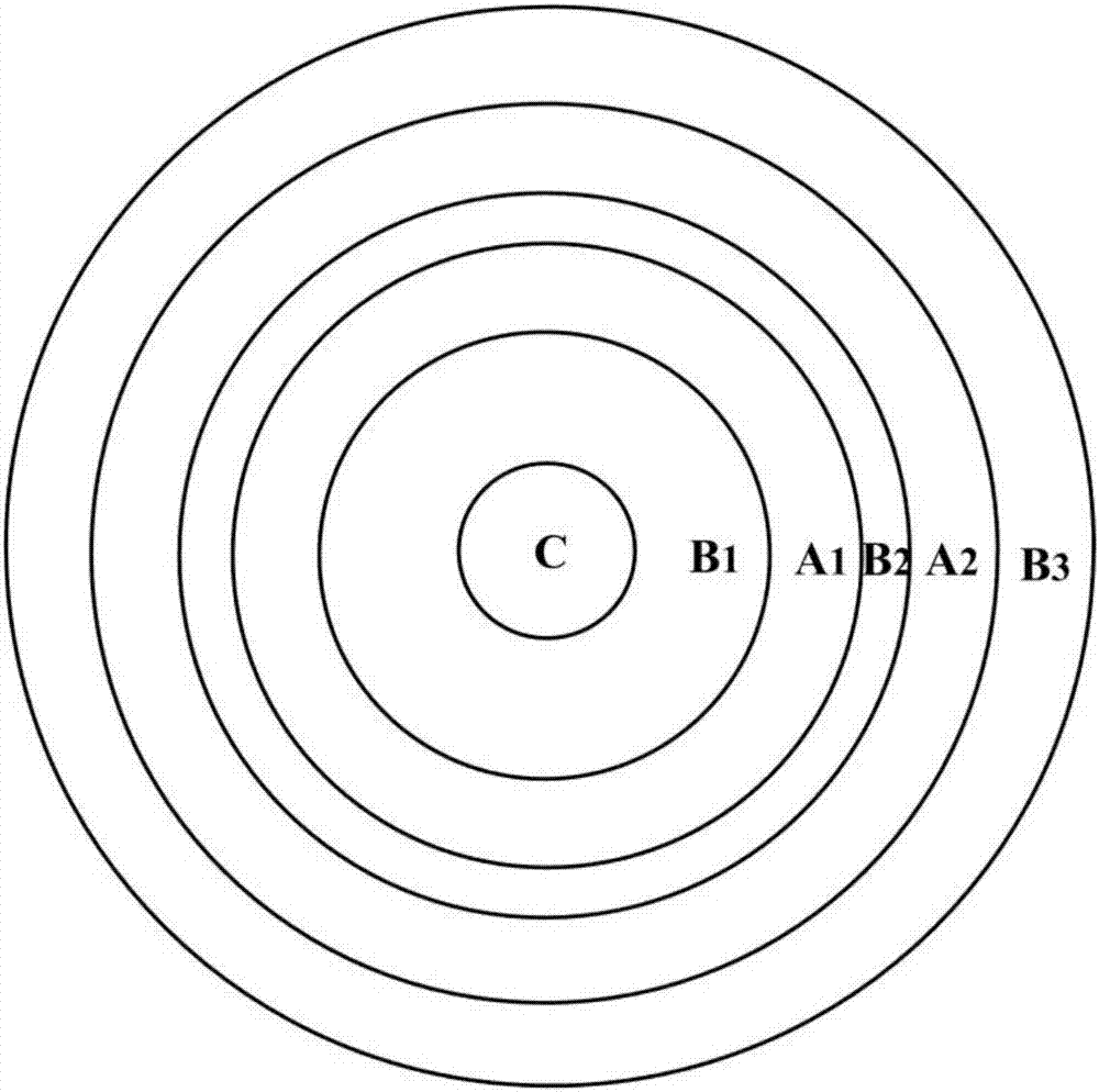
[0064] CdSe / ZnS / CdSe / ZnS (structure is C / B 1 / A 1 / B 2 ) synthesis of quantum dots:

[0065] Core C: Synthetic CdSe core with a particle size of about 3nm and a fluorescence emission peak of 580nm;

[0066] Shell B 1 : A monolayer of ZnS is coated on the CdSe core to obtain C / B 1 structured quantum dots;

[0067] Shell A 1 : Coating monolayer CdSe on C / B 1 structure of quantum dots, get C / B 1 / A 1 structured quantum dots;

[0068] Shell B 2 : Coating C / B with monolayer ZnS 1 / A 1 structure of quantum dots, the structure is C / B 1 / A 1 / B 2 quantum dots;

[0069] The quantum dot emits red light, the particle size is about 5nm, and the fluorescence peak is at 620nm.

Embodiment 2

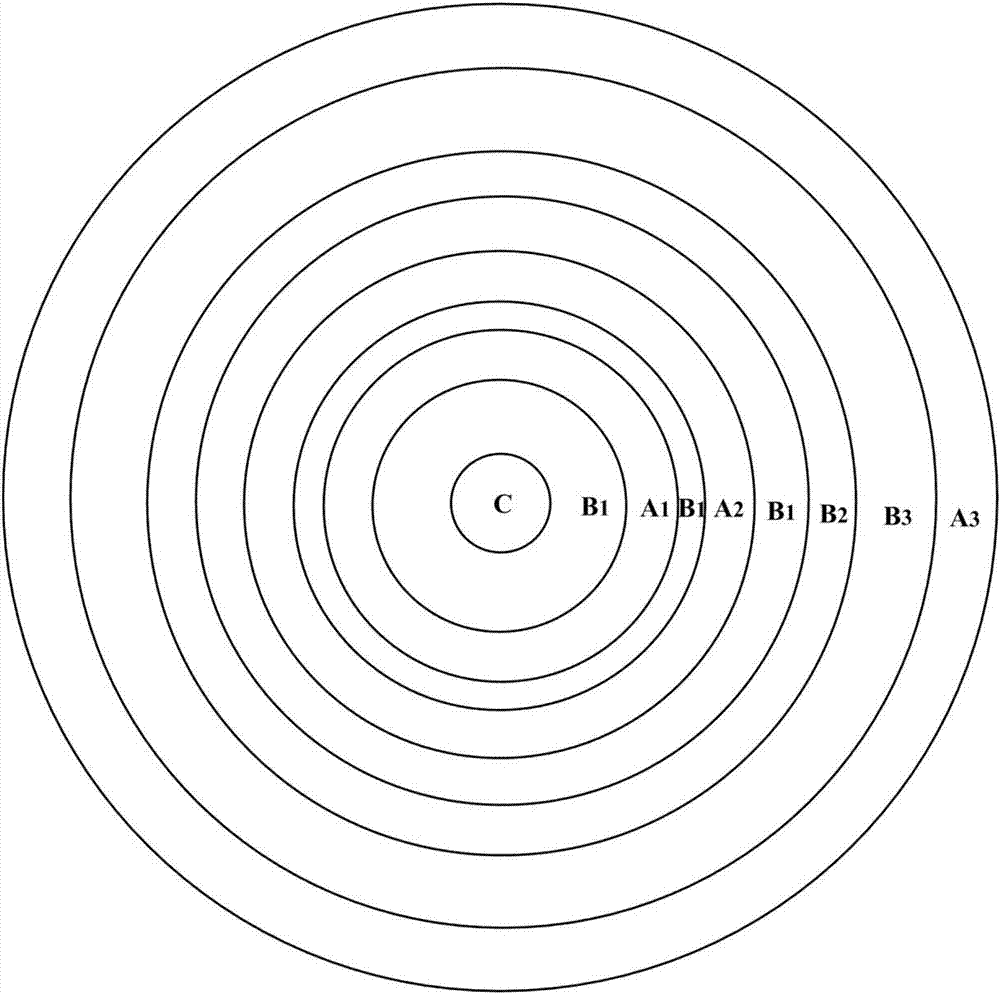
[0071] CdSe / CdS / ZnS / CdS / CdS / ZnS (structure is C / B 1 / B 2 / A 1 / B 1 / B 2 ) synthesis of quantum dots:

[0072] Core C: Synthetic CdSe core, the fluorescence emission peak is 580nm;

[0073] D. 1 Shell group (including B 1 / B 2 Shell layer): The monolayer CdS and ZnS are sequentially coated on the outer surface of the core C to obtain C / B 1 / B 2

[0074] structured quantum dots;

[0075] Shell A 1 : CdS monolayer coated on C / B 1 / B 2 The outer surface of the quantum dots of the structure, the obtained structure is C / B 1 / B 2 / A 1

[0076] structured quantum dots;

[0077] D. 2 Shell group (including B 1 / B 2 Shell layer): The monolayer CdS and ZnS are sequentially coated on the outer surface of the core C to obtain C / B 1 / B 2 / A 1 / B 1 / B 2 structured quantum dots;

[0078] The quantum dot emits red light with a fluorescence peak at 620nm.

Embodiment 3

[0080] Compared with Example 1, the manufacturing method of the quantum dots of this embodiment differs in that:

[0081] The position of the fluorescent peak of the synthesized CdSe core is at 520nm, in the second shell B 3 The outer layer is sequentially covered with the first shell layer and the second shell layer A 3 , B 4 、A 4 , B 5 、A 5 ,...,B 10 、A 10 , there are 20 shells in total, the total thickness of the shell is 20 monolayers, and the thickness of each layer is 1 monolayer, A 3 to A 10 Materials and Example 1 A 1 The materials are the same, the final luminous color is red light, and the particle size of the obtained quantum dots is about 20nm.


PUM

PropertyMeasurementUnit
particle diameteraaaaaaaaaa

Abstract

The invention provides a quantum dot, an ink and a quantum dot light emitting display device. The quantum dot of the core-shell structure includes C / B1 / A1...... / Bn / An / Bn+1 / An+1, or C / B1 / A1...... / Bn / An / Bn+1, wherein C is a core, B1 to Bn+1 shell layers are Class B shell layers, A1 to An+1 shell layers are Class A shell layers, the shell layers are arranged away from the C core in an ascending order, and the Class A shell layers and the Class B shell layers are crosswise arranged to form a plurality of adjacent A / B shell groups, n is an integer and n is greater than or equal to 1; the C core and the Class A shell layers are used for luminescence; in the C / B core shell group and any A / B shell group, the conduction band bottom of the B type shell layer is higher than the conduction band bottom of the A shell layer or the C core, and the valence band top of the B shell layer is lower than the valence band top of the A shell layer or the C core. Each shell layer of the quantum dot forms a multi-layer structure with alternating band gaps, and achieves the effect of improving the luminous efficiency while maintaining the stability of the quantum dots.

Description

technical field [0001] The present application relates to the field of quantum dot materials, in particular, to a quantum dot, ink and a quantum dot light-emitting display device. Background technique [0002] For the stability of quantum dots, traditional CdSe / CdS, CdSe / ZnS and other simple core / shell (core / shell) structures usually make the shell thicker, such as red light quantum dots with a diameter of 10nm CdSe / CdS structure, The core diameter is only about 3 nm. In this way, in the application of Quantum Dot Light Emitting Diodes (QLED), the quantum dots may still maintain good photoelectric properties after purification, ligand exchange and other treatments. However, the current life of QLED devices, especially the blue light, is still not ideal, and has not yet met the application requirements. To solve this problem, the quantum dots can be made thicker. In the prior art, large-size quantum dots of about 15nm are generally used as QLEDs to improve the device life. ...

Claims


Application Information

Patent Timeline
Patent Type & Authority Applications(China)
IPC IPC(8): H01L51/50C09D11/50
CPCC09D11/50H10K50/115
Inventor 谢松均
Owner NANJING TECH CORP LTD
Why Eureka
Try Eureka