Storage, formation method thereof and semiconductor device

A memory and conductor technology, applied in semiconductor devices, semiconductor/solid-state device manufacturing, and electric solid-state devices, etc., can solve the problems of high contact resistance, reduced component size, and high production costs.

Active Publication Date: 2017-10-10
CHANGXIN MEMORY TECH INC
View PDF5 Cites 14 Cited by
  • Summary
  • Abstract
  • Description
  • Claims
  • Application Information

AI Technical Summary

Problems solved by technology

[0004] With the continuous reduction of the size of the memory, the feature size of each component in the memory (for example, the line width of the word line conductor and the bit line, the opening size of the contact window, etc.) will be a great challenge
Moreover, when performing a multi-pass photolithography process, there is a problem of alignment deviation between different masks, so that after the multi-pass masks are superimposed on each other, the multiple displacement deviations of the corresponding multi-pass masks will be superimposed on each other, which will further affect the The electrical connection between some components in the memory affects the
Therefore, when the contact window of the storage node is directly defined by the photolithography process, a large displacement deviation will be generated between the formed storage node contact and the storage node contact area, and the contact resistance will be too large.
[0005] It can be seen that when the contact window corresponding to the contact area of ​​the storage node is directly defined by using the photolithography process to prepare the storage node contact, it is not only a problem of high manufacturing cost, but also the alignment accuracy of the multi-pass photolithography process is limited. , so that when multiple masks are superimposed on each other, a greater displacement deviation will occur
In this way, not only will the performance of the memory formed subsequently be affected, but it is also not conducive to the reduction of the size of the components.

Method used


Image

  • Storage, formation method thereof and semiconductor device
  • Storage, formation method thereof and semiconductor device
  • Storage, formation method thereof and semiconductor device

Examples


Embodiment 1

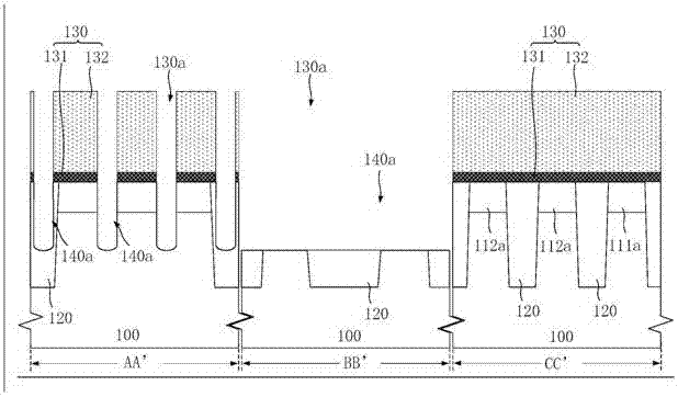
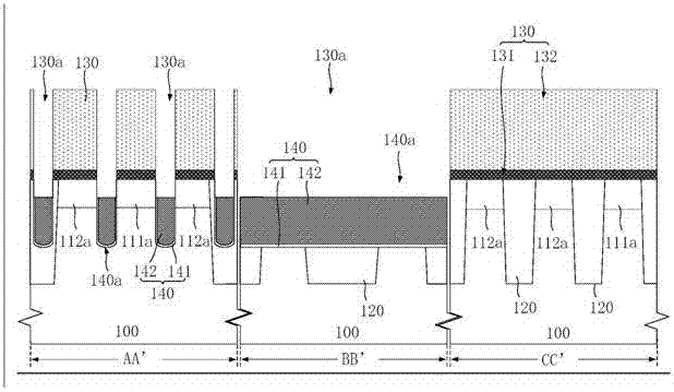
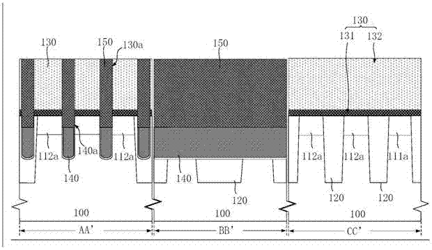
[0150] figure 1 It is a schematic flow chart of the forming method of the memory in Embodiment 1 of the present invention, such as figure 1 As shown, in the forming method of the memory shown in this embodiment, the contact window defined by the first isolation barrier and the second isolation barrier is directly used, and under the limitation of the first isolation barrier and the second isolation barrier, the A conductive layer is aligned and filled in the contact hole to form a storage node contact. Compared with the traditional method, in this embodiment, when defining the contact window corresponding to the storage node contact, it is not necessary to use an additional photolithography process. The following is attached figure 1 The method of forming the memory in this embodiment will be described in detail.

[0151] Figure 2a is a top view of the memory forming method in Embodiment 1 of the present invention when step S110 is executed, Figure 2b for Figure 2a Th...

Embodiment 2

[0206] The difference from Embodiment 1 is that in the memory forming method of this embodiment, the surface of the first isolation barrier corresponding to the word line conductor is higher than the surface of the second isolation barrier corresponding to the bit line, so that the first isolation barrier can be used to automatically A continuous conductive layer is formed in an aligned manner, and the conductive layer extends along the first direction, thereby facilitating adjustment of the extending direction of the storage node contact when the storage node contact is prepared. Compared with the traditional forming method, in this embodiment, there is no need to additionally form a redistribution layer to adjust the extension direction of the storage node contact by photolithography process, which is beneficial to simplify the process.

[0207] Figure 9 It is a schematic flow chart of the forming method of the memory in Embodiment 2 of the present invention, such as Figu...

Embodiment 3

[0231] The present invention also provides a memory in which a contact window corresponding to a storage node contact is directly defined by a first isolation barrier corresponding to a word line conductor and a second isolation barrier corresponding to a bit line, so that the defined The boundaries of the contact windows respectively extend to positions close to the bit line and close to the sidewalls of the word line conductors. Therefore, the projection of the contact window in the height direction can not only cover the second contact region, but also the projected area of ​​the contact window is larger than that of the second contact area. The projected area of ​​the second contact area in the height direction. In this way, on the one hand, the formed storage node contact can be completely electrically connected to the second contact region; on the other hand, there is a larger contact area between the storage node contact and the second contact region, which is beneficial...


PUM


Abstract

The invention provides a storage, a formation method thereof and a semiconductor device. A first isolation line covering a word line in a self-alignment way is used as a first isolation screen, a second isolation line covering the word line in a self-alignment way is utilized so that the second isolation line is combined with the word line to form a second isolation screen, and a contact window corresponding to a second contact area is defined by intersection of the first isolation screen and the second isolation screen. The contact window in contact with a corresponding storage node can be defined without a photoetching process, the fabrication cost is reduced, the alignment deviation among multiple steps of the photoetching process also can be reduced, and the contact resistance between the storage node formed subsequently and the second contact area is favorably improved.

Description

technical field [0001] The invention relates to the technical field of semiconductors, in particular to a memory, a method for forming the same, and a semiconductor device. Background technique [0002] A memory typically includes a storage capacitor for storing charge representing stored information and a storage transistor connected to the storage element. An active region, a drain region and a gate are formed in the memory transistor, the gate is used to control the flow of current between the source region and the drain region, and is connected to a word line conductor, and the source region is used to form The bit line contact area is used to connect to the bit line, and the drain area is used to form a storage node contact area to be connected to the storage capacitor. [0003] In the preparation method of traditional memory, generally include defining active area (Active Area, AA), defining word line conductor (Word Line, WL), defining bit line contact window, defini...

Claims


Application Information

Patent Timeline
Patent Type & Authority Applications(China)
IPC IPC(8): H01L27/108H01L21/8242
CPCH10B12/31H10B12/02H10B12/485H10B12/0335
Inventor 不公告发明人
Owner CHANGXIN MEMORY TECH INC
Why Eureka
Try Eureka