Semiconductor device and method of fabricating the same

a semiconductor and semiconductor technology, applied in semiconductor/solid-state device manufacturing, basic electric elements, electric devices, etc., can solve the problems of reducing film quality, reducing cost, and undesirable carrying out the photolithography process twice, so as to reduce the number of execution times of the photolithography process

Inactive Publication Date: 2008-01-01
KK TOSHIBA
View PDF5 Cites 6 Cited by
  • Summary
  • Abstract
  • Description
  • Claims
  • Application Information

AI Technical Summary

Benefits of technology

[0011]Therefore, an object of the present invention is to provide a semiconductor device in which the number of execution times of the photolithography process can be reduced by once but another step such as the hydrogen heat treatment need not be added, and a method of fabricating the semiconductor device.

Problems solved by technology

However, carrying out the photolithography process twice is undesirable from the viewpoint of cost reduction.
Accordingly, when a process in which a gate electrode is previously formed and separated by the forming of the element isolation regions, there is a possibility that the previously formed gate oxide film may be damaged by hydrogen anneal, whereupon the film quality may be reduced with the result of reduction in the reliability of elements.

Method used


Image

  • Semiconductor device and method of fabricating the same
  • Semiconductor device and method of fabricating the same
  • Semiconductor device and method of fabricating the same

Examples


Embodiment Construction

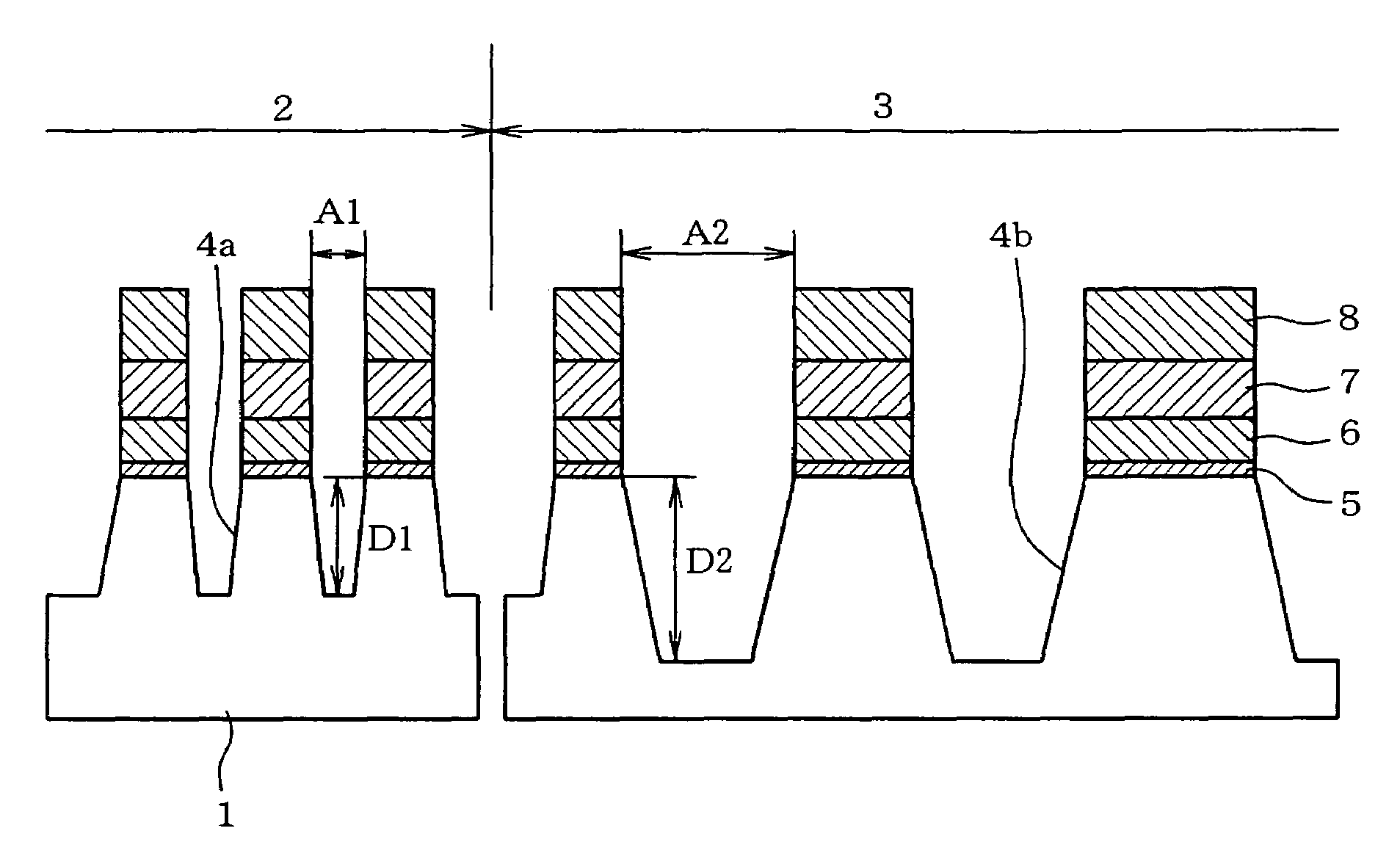
[0021]One embodiment of the present invention will be described with reference to the accompanying drawings. The invention is applied to a NAND flash memory in the embodiment. In a fabrication process of the NAND flash memory in the embodiment, trenches are formed in a semiconductor substrate which has previously been formed with part of film structure for a gate electrode. The structure of the semiconductor device in the trench forming steps and the fabrication process of the semiconductor device will hereinafter be described.

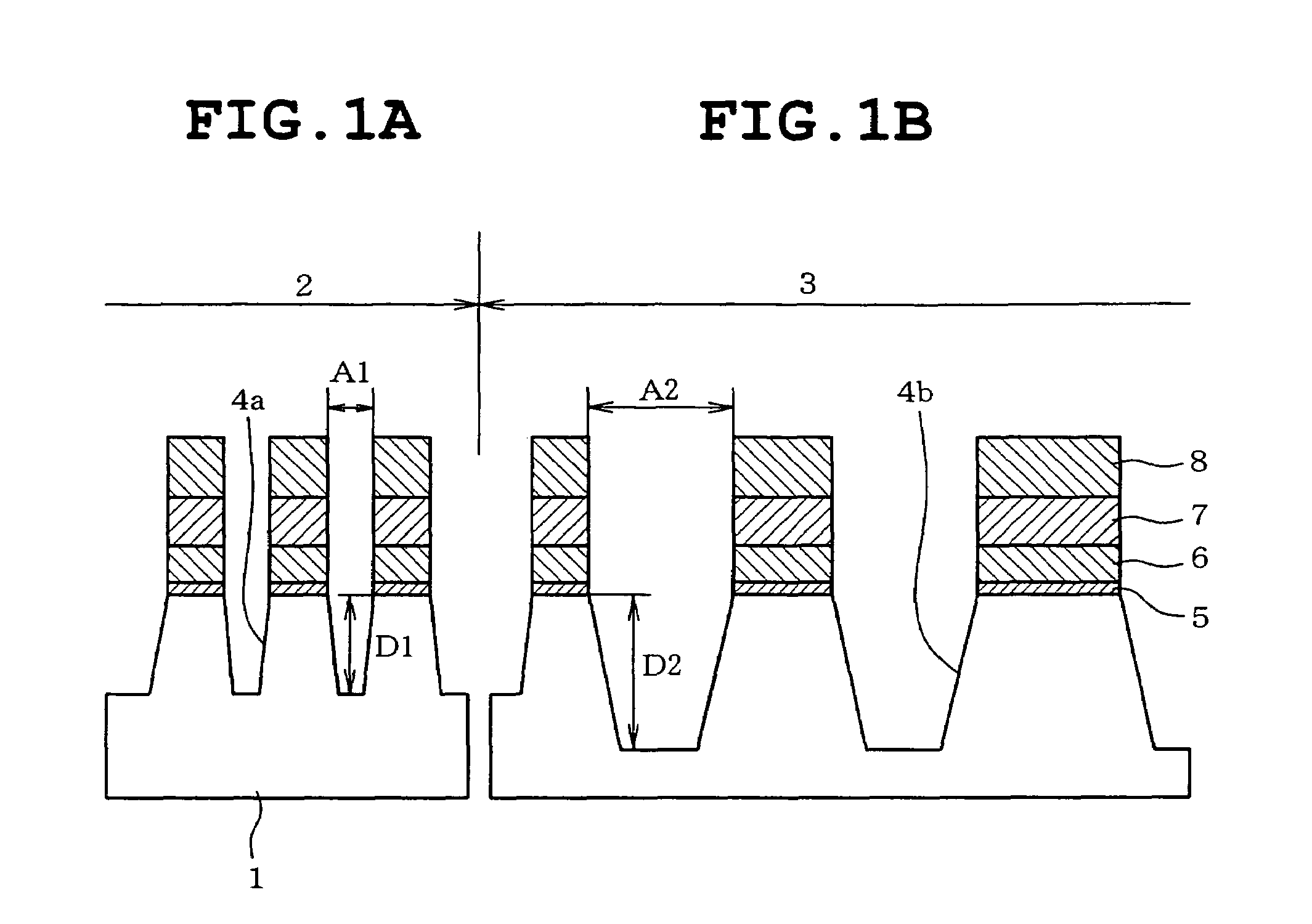
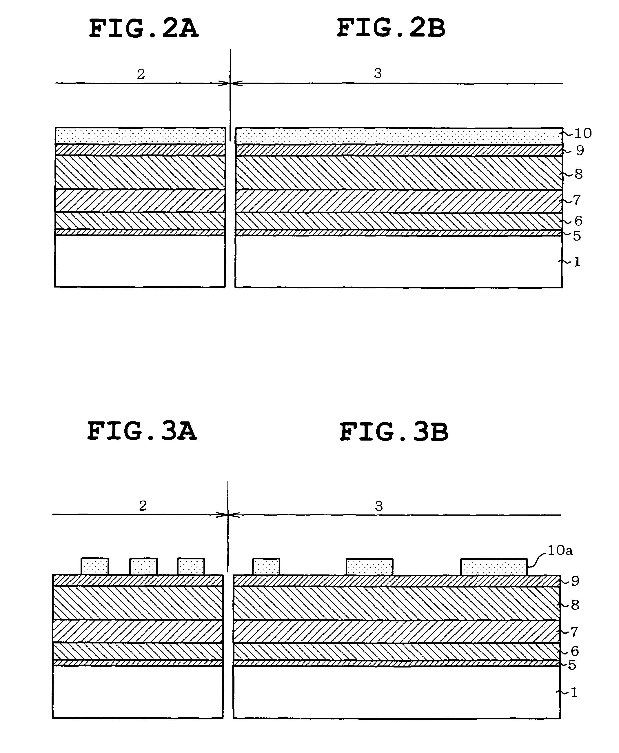
[0022]Referring to FIGS. 1A and 1B, schematic sectional views of the semiconductor device are shown. These views show the condition immediately after completion of an etching process. Trenches 4a and 4b are formed in a memory cell region 2 and a peripheral circuit region 3 so as to have different depths respectively. On an upper surface of the silicon substrate 1 are deposited a silicon oxide film 5 serving as a gate insulating film, a polycrystalline silicon ...


PUM

PropertyMeasurementUnit
temperatureaaaaaaaaaa
thicknessaaaaaaaaaa
thicknessaaaaaaaaaa

Abstract

A method of fabricating a semiconductor device includes forming a gate insulating film on an upper surface of a silicon substrate, forming a polycrystalline silicon film on the gate insulating film, and etching the polycrystalline silicon film, the gate insulating film, and the silicon substrate with a patterned coating type carbon film and a silicon nitride film so that first and second trenches are simultaneously formed. The first trench has a first width and a first depth and the second trench has a second width larger than the first width and the second depth larger than the first depth.

Description

CROSS-REFERENCE TO RELATED APPLICATIONS[0001]This application is based upon and claims the benefit of priority from the prior Japanese Patent Application No. 2004-207367, filed on Jul. 14, 2004, the entire contents of which are incorporated herein by reference.BACKGROUND OF THE INVENTION[0002]1. Field of the Invention[0003]The present invention relates to a semiconductor device having a plurality of trenches with different opening widths and a method of fabricating the semiconductor device.[0004]2. Description of the Related Art[0005]Semiconductor devices of the above-described type include a semiconductor storage device provided with a number of memory cell transistors, for example. One type of the memory cell transistor is formed with an element isolation region called “shallow trench isolation (STI)” in order that memory cell transistors and peripheral circuit transistors may electrically be isolated. The STI is formed by burying insulating films in a surface of a semiconductor s...

Claims


Application Information

Patent Timeline
Patent Type & Authority Patents(United States)
IPC IPC(8): H01L21/4763
CPCH01L21/76229
Inventor MATSUMOTO, TAKANORI
Owner KK TOSHIBA
Why Eureka
Try Eureka