Memory, method for forming the memory, and semiconductor device

A memory and conductor technology, applied in the direction of semiconductor devices, semiconductor/solid-state device manufacturing, electric solid-state devices, etc., can solve the problems of complex preparation process, increase the difficulty of memory preparation, and small photolithography process window, so as to simplify the process flow and save The effect of preparation cost and reduction of preparation difficulty

Active Publication Date: 2018-11-23
CHANGXIN MEMORY TECH INC
View PDF5 Cites 6 Cited by
  • Summary
  • Abstract
  • Description
  • Claims
  • Application Information

AI Technical Summary

Problems solved by technology

[0006] Therefore, in the existing methods for forming bit line contacts and storage node contacts, the preparation process is relatively complicated, and the photolithography process window is small, which increases the difficulty of memory preparation.

Method used


Image

  • Memory, method for forming the memory, and semiconductor device
  • Memory, method for forming the memory, and semiconductor device
  • Memory, method for forming the memory, and semiconductor device

Examples


Embodiment 1

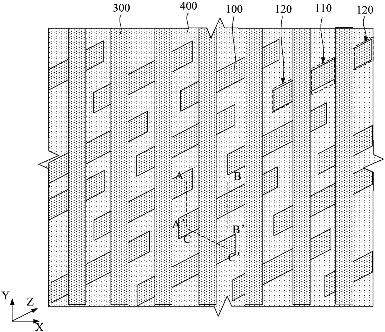
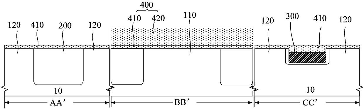
[0101] Figure 2a is a top view of the memory when step S100 is performed in the method for forming the memory in Embodiment 1 of the present invention, Figure 2b for Figure 2a Shown is the cross-sectional view of the memory along the directions AA', BB' and CC' when step S100 is performed in the method for forming the memory in Embodiment 1 of the present invention.

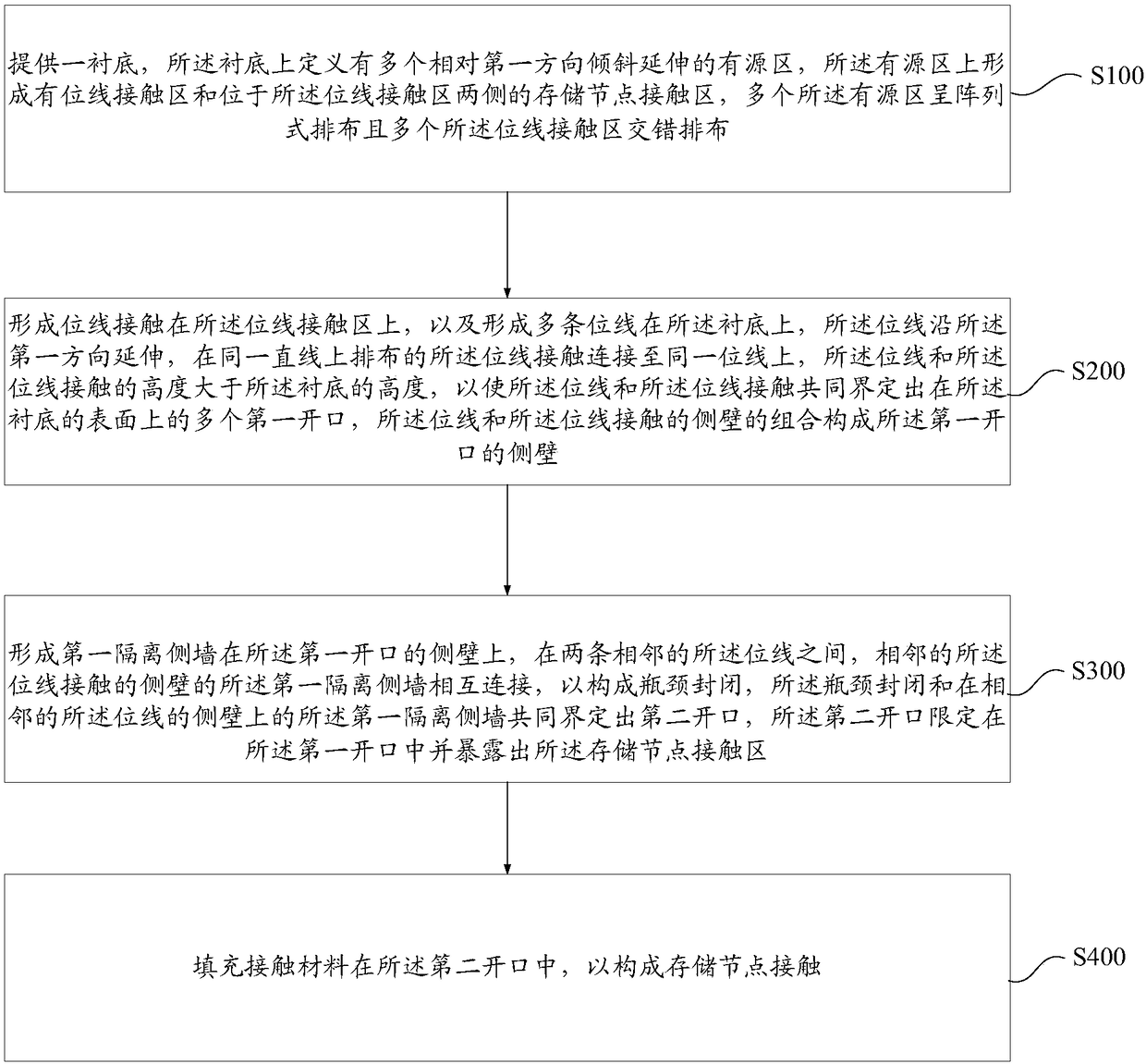
[0102] In step S100, specifically refer to Figure 2a and Figure 2b As shown, a substrate 10 is provided, and a plurality of active regions 100 extending obliquely relative to the first direction are defined on the substrate 10, and bit line contact regions 110 are formed on the active regions 100 and located on the active regions 100. For the storage node contact regions 120 on both sides of the bit line contact region 110, the first direction is the X direction shown in FIG. 2 , and the direction extending obliquely relative to the first direction is the Z direction shown in FIG. 2 . Further, an isolati...

Embodiment 2

[0155] Figure 12a is a top view of the memory in Embodiment 2 of the present invention, Figure 12b for Figure 12a Shown are cross-sectional views of the memory in Embodiment 2 of the present invention along the directions AA', BB' and CC'. Such as Figure 12a and Figure 12b As shown, the memory includes:

[0156] A substrate 10, defined on the substrate 10 to extend obliquely relative to the first direction (ie, Figure 12a shown in the Z direction) of the active region 100, the bit line contact region 110 and the storage node contact region 120 located on both sides of the bit line contact region 110 are formed on the active region 100; it should be noted that, Figure 12a only schematically shows several active regions 100;

[0157] a plurality of bit line contacts 510, formed on the bit line contact region 110 and in contact with the bit line contact region 110;

[0158] A plurality of bit lines 500 extending along the first direction (ie, Figure 12a X directio...

Embodiment 3

[0177] In addition, based on the memory described above, the present invention also provides a semiconductor device. In the field of semiconductors, it is usually necessary to form a corresponding lead-out terminal in contact with the lead-out region when the lead-out region is pulled out, so that the lead-out region can be controlled and led out through the lead-out terminal. And when multiple different lead-out areas need to be led out, it should also be ensured that the uncorresponding lead-out terminals are isolated from each other, so as to avoid the problem of signal crosstalk.

[0178] Based on this, the present invention provides a semiconductor device, which has at least two different lead-out regions, that is, a first contact region and a second contact region. A first conductor contact is formed on the first contact area, and an opening is defined by the sidewall of the first conductor contact after the first conductor contact is formed, and a corresponding opening ...


PUM


Abstract

The present invention provides a memory, a method for forming the memory and a semiconductor device. A first isolation sidewall is formed on a sidewall thereof by using the formed bit line and the bitline contact, and in the adjacent two bit lines, the first isolation sidewalls on the two nearest bit line contacts are connected to each other, so as to form a bottleneck closure, the opening formedby the isolation side wall and the bottleneck closure can be self-aligned to define the forming area of the storage node contact, so that only the operation of filling the opening with contact material is needed when the storage node contact is formed, and the photolithography process is not required. Thus, the execution times of the photolithography process can be reduced, the process flow is effectively simplified, the limitation of the photolithography process window can be avoided, and the preparation difficulty of the memory can be reduced.

Description

technical field [0001] The present invention relates to the technical field of semiconductors, in particular to a memory, a method for forming the same, and a semiconductor device. Background technique [0002] A memory typically includes a storage capacitor for storing charge representing stored information and a storage transistor connected to the storage element. Formed in the memory transistor are an active region, a drain region, and a gate, the gate controlling current flow between the source region and the drain region, and the source region constituting a bit line contact region for connecting to a bit line. line, and the drain region is used to form a storage node contact region to be connected to the storage capacitor. [0003] Wherein, a bit line contact needs to be formed on the bit line contact area, and then connected to the bit line through the bit line contact, and a storage node contact needs to be formed on the storage node contact area, and then connected...

Claims


Application Information

Patent Timeline
Patent Type & Authority Applications(China)
IPC IPC(8): H01L21/8242H01L27/108
CPCH10B12/315H10B12/485H10B12/0335H10B12/482
Inventor 不公告发明人
Owner CHANGXIN MEMORY TECH INC
Why Eureka
Try Eureka